ZHCSIK0A July   2018  – October 2021 TPS3430

PRODUCTION DATA  

  1. 特性
  2. 应用
  3. 说明
  4. Revision History
  5. Pin Configuration and Functions
  6. Specifications
    1. 6.1 Absolute Maximum Ratings
    2. 6.2 ESD Ratings
    3. 6.3 Recommended Operating Conditions
    4. 6.4 Thermal Information
    5. 6.5 Electrical Characteristics
    6. 6.6 Timing Requirements
    7. 6.7 Timing Diagrams
    8. 6.8 Typical Characteristics
  7. Detailed Description
    1. 7.1 Overview
    2. 7.2 Functional Block Diagrams
    3. 7.3 Feature Description
      1. 7.3.1 CRST
      2. 7.3.2 Window Watchdog
        1. 7.3.2.1 SET0 and SET1
          1. 7.3.2.1.1 Enabling the Window Watchdog
          2. 7.3.2.1.2 Disabling the Watchdog Timer When Using the CRST Capacitor
          3. 7.3.2.1.3 SET0 and SET1 During Normal Watchdog Operation
      3. 7.3.3 Window Watchdog Timer
        1. 7.3.3.1 CWD
        2. 7.3.3.2 WDI Functionality
        3. 7.3.3.3 WDO Functionality
    4. 7.4 Device Functional Modes
      1. 7.4.1 VDD is Below VPOR ( VDD < VPOR)
      2. 7.4.2 VDD is Above VPOR And Below VDD (min)( VPOR < VDD < VDD (min))
      3. 7.4.3 Normal Operation (VDD ≥ VDD (min))
  8. Application and Implementation
    1. 8.1 Application Information
      1. 8.1.1 CRST Delay
        1. 8.1.1.1 Factory-Programmed Watchdog Reset Delay Timing
        2. 8.1.1.2 CRST Programmable Watchdog Reset Delay
      2. 8.1.2 CWD Functionality
        1. 8.1.2.1 Factory-Programmed Timing Options
        2. 8.1.2.2 CWD Adjustable Capacitor Watchdog Timeout
    2. 8.2 Typical Applications
      1. 8.2.1 Monitoring Microcontroller with Watchdog Timer - Design 1
        1. 8.2.1.1 Design Requirements - Design 1
        2. 8.2.1.2 Detailed Design Procedure - Design 1
          1. 8.2.1.2.1 Meeting the Minimum Watchdog Reset Delay - Design 1
          2. 8.2.1.2.2 Setting the Watchdog Window - Design 1
          3. 8.2.1.2.3 Calculating the WDO Pull-up Resistor - Design 1
      2. 8.2.2 Monitoring Microcontroller with a Programmed Window Watchdog Timer - Design 2
        1. 8.2.2.1 Design Requirements - Design 2
        2. 8.2.2.2 Detailed Design Procedure - Design 2
          1. 8.2.2.2.1 Meeting the Minimum Watchdog Reset Delay - Design 2
          2. 8.2.2.2.2 Setting the Watchdog Window - Design 2
          3. 8.2.2.2.3 Calculating the WDO Pull-up Resistor - Design 2
      3. 8.2.3 Monitoring Microcontroller with a Latching Window Watchdog Timer - Design 3
        1. 8.2.3.1 Design Requirements - Design 3
        2. 8.2.3.2 Detailed Design Procedure - Design 3
          1. 8.2.3.2.1 Meeting the Latching Output Requirement - Design 3
          2. 8.2.3.2.2 Setting the Watchdog Window - Design 3
        3. 8.2.3.3 Application Curve - Design 3
  9. Power Supply Recommendations
  10. 10Layout
    1. 10.1 Layout Guidelines
    2. 10.2 Layout Example
  11. 11Device and Documentation Support
    1. 11.1 Device Support
    2. 11.2 Documentation Support
      1. 11.2.1 Related Documentation
    3. 11.3 接收文档更新通知
    4. 11.4 支持资源
    5. 11.5 Trademarks
    6. 11.6 Electrostatic Discharge Caution
    7. 11.7 术语表
  12. 12Mechanical, Packaging, and Orderable Information

封装选项

机械数据 (封装 | 引脚)
散热焊盘机械数据 (封装 | 引脚)
订购信息
Disabling the Watchdog Timer When Using the CRST Capacitor

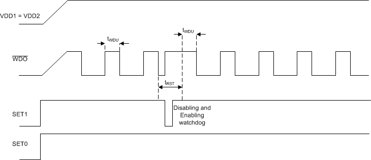
When using the TPS3430 with fixed timing options, if the watchdog is disabled and reenabled while WDO is asserted (logic low) the watchdog performs as described in the Section 7.3.2.1.1 section. However, if there is a capacitor on the CRST pin, and the watchdog is disabled and reenabled when WDO is asserted (logic low), then the watchdog behaves as shown in Figure 7-3. When the watchdog is disabled, WDO goes high impedance (logic high). However, when the watchdog is enabled again, the tRST period must expire before the watchdog resumes normal operation.
GUID-7907FFE6-8EA6-4C31-84C4-E02B5DA9D7BB-low.gif
There is no WDI signal in this figure, WDI is always at GND.
Figure 7-3 Enabling and Disabling the Watchdog Timer During a WDO Reset Event