ZHCSHV0C June 2017 – April 2018 TPS2595
PRODUCTION DATA.
- 1 特性
- 2 应用
- 3 说明
- 4 修订历史记录
- 5 Device Comparison Table
- 6 Pin Configuration and Functions
- 7 Specifications
-
8 Detailed Description
- 8.1 Overview
- 8.2 Functional Block Diagram
- 8.3 Feature Description
- 8.4 Device Functional Modes
-
9 Application and Implementation
- 9.1 Application Information
- 9.2
Typical Application
- 9.2.1 Design Requirements
- 9.2.2 Detailed Design Procedure
- 9.2.3 Support Component Selection: CIN
- 9.2.4 Application Curves
- 9.2.5 Controlled Power Down (Quick Output Discharge) using TPS2595x5
- 9.2.6 Overvoltage Lockout using TPS259573
- 10Power Supply Recommendations
- 11Layout
- 12器件和文档支持
- 13机械、封装和可订购信息
9.2.5 Controlled Power Down (Quick Output Discharge) using TPS2595x5
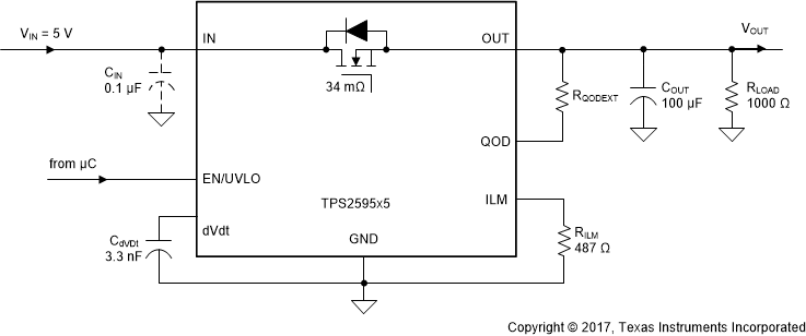
When the TPS2595x5 device is disabled, the output voltage is left floating and the power-down profile is entirely dictated by the load. In some applications, this can lead to undesired activity because the load is not powered down to a defined state. Controlled output discharge can ensure the load is completely turned off and is not in an undefined operational state. The QOD pin in the TPS2595x5 device can be connected to the OUT pin to facilitate the Quick Output Discharge function, as shown in Figure 62. When the TPS2595x5 device is disabled, the QOD pin is pulled low and provides a quick discharge path for the output capacitor. The output voltage discharge rate is dictated by the output capacitor COUT, the total discharge path resistance (internal plus external), and the load.
 Figure 62. Circuit Implementation with Quick Output Discharge Function using TPS2595x5
![TPS2595 Output Voltage Discharge using TPS259535 without QOD [VIN = 5 V, EN = H → L, COUT = 100 µF, RLOAD = 1000 Ω, RQODEXT = OPEN] TPS2595 tps2595x-output-voltage-discharge-using-tps259535-without-qod-scope-shot.gif](/ods/images/ZHCSHV0C/tps2595x-output-voltage-discharge-using-tps259535-without-qod-scope-shot.gif) Figure 63. Output Voltage Discharge using TPS259535 without QOD [VIN = 5 V, EN = H → L, COUT = 100 µF, RLOAD = 1000 Ω, RQODEXT = OPEN]
Figure 63. Output Voltage Discharge using TPS259535 without QOD [VIN = 5 V, EN = H → L, COUT = 100 µF, RLOAD = 1000 Ω, RQODEXT = OPEN]
![TPS2595 Output Voltage Discharge using TPS259535 with QOD [VIN = 5 V, EN = H → L, COUT = 100 µF, RLOAD = 1000 Ω, RQODEXT = Short] TPS2595 tps2595x-output-voltage-discharge-using-tps259535-with-qod-scope-shot.gif](/ods/images/ZHCSHV0C/tps2595x-output-voltage-discharge-using-tps259535-with-qod-scope-shot.gif) Figure 64. Output Voltage Discharge using TPS259535 with QOD [VIN = 5 V, EN = H → L, COUT = 100 µF, RLOAD = 1000 Ω, RQODEXT = Short]
Figure 64. Output Voltage Discharge using TPS259535 with QOD [VIN = 5 V, EN = H → L, COUT = 100 µF, RLOAD = 1000 Ω, RQODEXT = Short]