ZHCSCJ3D June 2014 – October 2017 TPS25942A , TPS25942L , TPS25944A , TPS25944L
UNLESS OTHERWISE NOTED, this document contains PRODUCTION DATA.
- 1 特性
- 2 应用范围
- 3 说明
- 4 修订历史记录
- 5 Device Comparison Table
- 6 Pin Configuration and Functions
- 7 Specifications
- 8 Parameter Measurement Information
-
9 Detailed Description
- 9.1 Overview
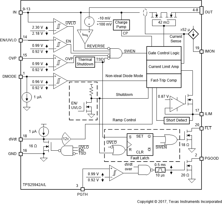
- 9.2 Functional Block Diagram
- 9.3
Feature Description
- 9.3.1 Enable and Adjusting Undervoltage Lockout
- 9.3.2 Overvoltage Protection (OVP)
- 9.3.3 Hot Plug-In and In-Rush Current Control
- 9.3.4 Overload and Short Circuit Protection
- 9.3.5 Reverse Current Protection
- 9.3.6 FAULT Response
- 9.3.7 Current Monitoring
- 9.3.8 Power Good Comparator
- 9.3.9 IN, OUT and GND Pins
- 9.3.10 Thermal Shutdown
- 9.4 Device Functional Modes
-
10Application and Implementation
- 10.1 Application Information
- 10.2
Typical Application
- 10.2.1 Design Requirements
- 10.2.2
Detailed Design Procedure
- 10.2.2.1 Step by Step Design Procedure
- 10.2.2.2 Programming the Current-Limit Threshold: R(ILIM) Selection
- 10.2.2.3 Undervoltage Lockout and Overvoltage Set Point
- 10.2.2.4 Programming Current Monitoring Resistor—RIMON
- 10.2.2.5 Setting Output Voltage Ramp Time (tdVdT)
- 10.2.2.6 Programing the Power Good Set Point
- 10.2.2.7 Support Component Selections—R6, R7 and CIN
- 10.2.3 Application Curves
- 10.3 System Examples
- 11Power Supply Recommendations
- 12Layout
- 13器件和文档支持
- 14机械、封装和可订购信息
9 Detailed Description
9.1 Overview
The TPS25942, TPS25944 is an eFuse Power Mux with integrated back-to-back FETs and enhanced built-in protection circuitry. It provides robust protection for all systems and applications powered from 2.7 V to 18 V.
For hot-plug-in boards, the device provides hot-swap power management with in-rush current control and programmable output ramp-rate. The device integrates overcurrent and short circuit protection. The precision overcurrent limit helps to minimize over design of the input power supply, while the fast response short circuit protection immediately isolates the load from input when a short circuit is detected. The device allows the user to program the overcurrent limit threshold between 0.6 A and 5.3 A via an external resistor.
The device provides precise monitoring of voltage bus for brown-out and overvoltage conditions and asserts fault for downstream system. Its overall threshold accuracy of 2% ensures tight supervision of bus, eliminating the need for a separate supply voltage supervisor chip. The TPS25942, TPS25944 is designed to control redundant power supply systems. The devices monitor V(IN) and V(OUT) to provide true reverse blocking from output when reverse condition or input power fail condition is detected. Also, a pair of the TPS25942 or TPS25944 devices can be configured to assign priority to the main power supply over the auxiliary power supply.
The additional features include:
- Precise current monitor output for health monitoring of the system
- Additional power good comparator with precision internal reference for output or any other rail voltage monitoring
- Electronic circuit breaker operation with overload timeout – TPS25944 only
- Over temperature protection to safely shutdown in the event of an overcurrent event
- De-glitched fault reporting for brown-out and overvoltage faults
- A choice of latched or automatic restart mode
9.2 Functional Block Diagram
9.3 Feature Description
9.3.1 Enable and Adjusting Undervoltage Lockout
The EN/UVLO pin controls the ON and OFF state of the internal FET. A voltage V(EN/UVLO) < V(ENF) on this pin turns off the internal FET, thus disconnecting IN from OUT, while voltage below 0.6 V takes the device into shutdown mode, with IQ less than 20 µA to ensure minimal power loss. Cycling EN/UVLO low and then back high resets the TPS2594xL that has latched off due to a fault condition.
The internal de-glitch delay on EN/UVLO falling edge is kept low for quick detection of power failure. For applications where a higher de-glitch delay on EN/UVLO is desired, or when the supply is particularly noisy, it is recommended to use an external bypass capacitor from EN/UVLO terminal to GND.
The undervoltage lock out can be programmed by using an external resistor divider from supply IN terminal to EN/UVLO terminal to GND as shown in Figure 50. When an undervoltage or input power fail event is detected, the internal FET is quickly turned off, and FLT is asserted. If the Under-Voltage Lock-Out function is not needed, the EN/UVLO terminal must be connected to the IN terminal. EN/UVLO terminal must not be left floating.
The device also implements internal undervoltage-lockout (UVLO) circuitry on the IN terminal. The device disables when the IN terminal voltage falls below internal UVLO Threshold V(UVF). The internal UVLO threshold has a hysteresis of 115 mV.
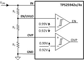 Figure 50. UVLO and OVP Thresholds Set By R1, R2 and R3
9.3.2 Overvoltage Protection (OVP)
The device incorporates circuit to protect system during overvoltage conditions. A resistor divider connected from the supply to OVP terminal to GND (as shown in Figure 50) programs the overvoltage threshold. A voltage more than V(OVPR) on OVP pin turns off the internal FET and protects the downstream load. This pin must be tied to GND when not used.
9.3.3 Hot Plug-In and In-Rush Current Control
The device is designed to control the in-rush current upon insertion of a card into a live backplane or other "hot" power source. This limits the voltage sag on the backplane’s supply voltage and prevents unintended resets of the system power. A slew rate controlled start-up (dVdT) also helps to eliminate conductive and radiative interferences. An external capacitor connected from the dVdT pin to GND defines the slew rate of the output voltage at power-on (as shown in Figure 51). Equation governing slew rate at start-up is shown in Equation 1.
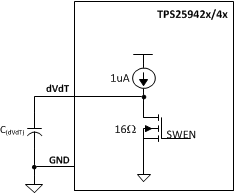 Figure 51. Output Ramp Up Time tdVdT is Set by C(dVdT)

where
- I(dVdT) = 1 µA (typical)
-
 = Desired output slew rate
 - GAIN(dVdT) = dVdT to OUT gain = 12
The total ramp time (tdVdT) of V(OUT) for 0 to V(IN) can be calculated using Equation 2.
The inrush current, I(INRUSH) can be calculated as shown in Equation 3.
The dVdT pin can be left floating to obtain a predetermined slew rate (tdVdT) on the output. When terminal is left floating, the device sets an internal ramp rate of 30 V/ms for output (V(OUT)) ramp.
Figure 61 and Figure 62 illustrate the inrush current control behavior of the TPS25942, TPS25944. For systems where load is present during start-up, the current never exceeds the overcurrent limit set by R(ILIM) resistor for the application. For defining appropriate charging time/rate under different load conditions, see the Setting Output Voltage Ramp Time (tdVdT) section.
9.3.4 Overload and Short Circuit Protection
The device monitors load current by sensing the voltage across the internal sense resistor. The FET current is monitored at both the start-up and during normal operation. During overload events, the device keeps the over current limited to the overcurrent limit (I(LIM)) programmed by R(ILIM) resistor as shown in Equation 4.

where
- I(LIM) is overload current limit in Ampere.
- R(ILIM) is the current limit resistor in kΩ
The device incorporates two distinct levels: an overcurrent-limit (I(LIM)) and a fast-trip threshold (I(FASTRIP)). The illustration of fast trip and current limit operation is shown in Figure 52.
Since the bias current on ILIM pin directly controls the current-limiting behavior of the device, the PCB routing of this node must be kept away from any noisy (switching) signals.
9.3.4.1 Overload Protection
During overload conditions, the internal current-limit amplifier in the TPS25942 regulates the output current to I(LIM). The output voltage droops during current regulation, resulting in increased device power dissipation. If the device junction temperature reaches the thermal shutdown threshold (T(TSD)), the internal FET is turned off. Once in thermal shutdown, The TPS25942L and 44L version stays latched off, whereas the TPS25942A and 44A commences an auto-retry cycle 128 ms after TJ < [T(TSD) – 12°C]. During thermal shutdown, the fault pin FLT pulls low to signal a fault condition. Figure 65 and Figure 66 illustrate the behavior of the system for overload conditions in the TPS25942.
The TPS25944 allows the overload current to flow through the device until I(LOAD) < I(FASTRIP). It starts the timer when I(LIM) < I(LOAD) < I(FASTRIP), and once the timer exceeds tCB(dly), the internal FET is turned off and FLT is asserted.
9.3.4.2 Short Circuit Protection
During a transient short circuit event, the current through the device increases very rapidly. As current-limit amplifier cannot respond quickly to this event due to its limited bandwidth, the device incorporates a fast-trip comparator, with a threshold I(FASTRIP). This comparator shuts down the pass device within 1 µs, when the current through internal FET exceeds I(FASTRIP) (I(OUT) > I(FASTRIP)), and terminates the rapid short-circuit peak current. The trip threshold is set to more than 50% of the programmed overload current limit (I(FASTRIP) = 1.5 × I(LIM) + 0.375). The fast-trip circuit holds the internal FET off for only a few microseconds, after which the device turns back on slowly, allowing the current-limit loop to regulate the output current to I(LIM). Then, device behaves similar to overload condition. Figure 67 through Figure 69 illustrate the behavior of the system when the current exceeds the fast-trip threshold.
9.3.4.3 Start-Up With Short on Output
During start-up with short, the device limits the current to I(LIM) and behaves similar to the overload condition afterwards. Figure 70 and Figure 71 illustrate the behavior of the device for start-up with short on the output. This feature helps in quick isolation of the fault and hence ensures stability of the DC bus.
9.3.4.4 Constant Current Limit Behavior During Overcurrent Faults
If during current limit, power dissipation of the internal FET PD = (V(IN) – V(OUT)) × I(OUT)] exceeds 10 W, there is an approximately 0% to 5% thermal fold back in the current limit value so that I(LIM) drops to IOS. Eventually, the device shuts down due to over temperature.
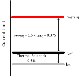 Figure 52. Fast-Trip Current
9.3.5 Reverse Current Protection
A fast reverse comparator controls the internal FET and turns off the FET whenever the output voltage V(OUT) exceeds the input voltage V(IN) by 10 mV (typical) for 1 μs (typical). This prevents damage to the devices on the input side of the TPS2594xx by preventing significant current from sinking into the input side. However, a reverse current of (V(OUT) - V(IN))/ RON) should flow from the output to the input to establish reverse voltage V(REVTH) of –10 mV across the device. The typical value of reverse current, needed for reverse voltage detection is –10 mV/ 42 mΩ = –238 mA
In power muxing applications, the reverse current magnitude I(REV) depends on the slew-rate of the output voltage V(OUT) and the system input capacitance CIN as shown in Equation 5.

For example, if the ramp rate of the output voltage is set at 10 mV/ μs then the required input capacitance CIN to achieve reverse current greater than 238 mA is 23.8 µF. Considering tolerance of ±10% in capacitance and a standard value, capacitor of 33 µF should be used as CIN in this case.
9.3.6 FAULT Response
The FLT open-drain output is asserted (active low) during undervoltage, overvoltage, reverse voltage-current and thermal shutdown conditions. Additionally, in the TPS25944, the FLT is asserted when overload condition exists for more than the fault time period (tCB(dly)). The FLT signal remains asserted until the fault condition is removed and the device resumes normal operation. The device is designed to eliminate false fault reporting by using an internal "de-glitch" circuit for undervoltage and overvoltage (2.2-µs typical) conditions without the need for external circuitry. This ensures that fault is not accidentally asserted during transients on input bus.
Connect FLT with a pull up resistor to Input or Output voltage rail. FLT may be left open or tied to ground when not used. V(IN) falling below V(UVF) = 2.1 V resets FLT.
9.3.7 Current Monitoring
The current source at IMON terminal is configured to be proportional to the current flowing from IN to OUT. This current can be converted to a voltage using a resistor R(IMON) from IMON terminal to GND terminal. This voltage, computed using Equation 7, can be used as a means of monitoring current flow through the system.
The maximum voltage range for monitoring the current (V(IMONmax)) is limited to minimum([V(IN) – 2.2 V], 6 V) to ensure linear output. This puts limitation on maximum value of R(IMON) resistor and is determined by Equation 6.

The output voltage at IMON terminal is calculated from Equation 7.

where
- GAIN(IMON) = Gain factor I(IMON):I(OUT) = 52 µA/A
- I(OUT) = Load current
- I(IMON_OS) = 0.8 µA (typical)
This pin must not have a bypass capacitor to avoid delay in the current monitoring information.
The voltage at IMON pin can be digitized using an ADC (such as ADS1100, SBAS239) to read the current monitor information over an I2C bus.
9.3.8 Power Good Comparator
The devices incorporate a Power Good comparator for co-ordination of status to downstream DC-DC converters or system monitoring circuits. The comparator has an internal reference of V(PGTHR) = 0.99 V at negative terminal and positive terminal PGTH can be utilized for monitoring of either input or output of the device. The comparator output PGOOD is an open-drain active high signal, which can be used to indicate the status to downstream units. PGOOD is asserted high when internal FET is fully enhanced and PGTH pin voltage is higher than internal reference V(PGTHR).
The PGOOD signal has deglitch time incorporated to ensure that internal FET is fully enhanced before heavy load is applied by downstream converters. Rising deglitch delay is determined by Equation 8.
Connect the PGOOD pin with a pull up resistor to Input or Output voltage rail. PGOOD may be left open or tied to ground when not used.
9.3.9 IN, OUT and GND Pins
The device has multiple pins for input (IN) and output (OUT).
All IN pins must be connected together and to the power source. A ceramic bypass capacitor close to the device from IN to GND is recommended to alleviate bus transients. The recommended operating voltage range is 2.7 V-18 V.
Similarly all OUT pins must be connected together and to the load. V(OUT) in the ON condition, is calculated using Equation 9.

where, RON is the total ON resistance of the internal FET.
GND terminal is the most negative voltage in the circuit and is used as a reference for all voltage reference unless otherwise specified.
9.3.10 Thermal Shutdown
The device has built-in over temperature shutdown circuitry designed to disable the internal FET, if the junction temperature exceeds 160°C (typical). The TPS25942L, 44L version latches off the internal FET, whereas the TPS25942A, 44A commences an auto-retry cycle 128 ms after TJ < [T(TSD) – 12°C]. During the thermal shutdown, the fault pin FLT pulls low to signal a fault condition.
9.4 Device Functional Modes
9.4.1 Diode Mode
The device provides a Diode Mode, where the power path from IN to OUT acts as a non-ideal diode rather than a FET, as shown in Figure 53. This mode is activated through DMODE terminal. This is an active high terminal with internal pull-down. The terminal is useful in Power-Mux applications to switch over from master to slave supplies and vice-versa smoothly, when two supplies are within a diode drop of each other. A high at this terminal activates the non-ideal diode mode. In this mode, the circuit breaker functionality (TPS25944x) is disabled and the overload current limit is set to 50 % of current limit determined by R(ILIM) resistor.
 Figure 53. Diode Mode: IN to OUT Power Path
9.4.2 Shutdown Control
The internal FET and hence the load current can be remotely switched off by taking the UVLO pin below its 0.6 V threshold with an open collector or open drain device as shown in Figure 54. The device quiescent current is reduced to less than 20 µA in this state. Upon releasing the UVLO pin the device turns on with soft-start cycle.
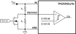 Figure 54. Shutdown Control
9.4.3 Operational Differences Between the TPS25942 and TPS25944
The TPS25942 and TPS25944 respond differently to overload and short circuit conditions. The operational differences are explained in Table 1.
Table 1. Device Operational Differences
| Device | TPS25942 (Current Limiter) |
TPS25944 (Circuit Breaker) |
|---|---|---|
| Start-up | Inrush ramp controlled by dVdT | Inrush ramp controlled by dVdT |
| Inrush limited to I(LIM) level as set by R(ILIM) | Inrush limited to I(LIM) level as set by R(ILIM) | |
| Fault Timer runs when current is limited to I(LIM) | ||
| Fault timer expires after tCB(dly) (4 ms) causing device shutoff | ||
| If TJ > T(TSD) device shuts off | Device turns off if TJ > T(TSD) before timer expires | |
| Over current response | Current is limited to I(LIM) level as set by R(ILIM) | Current is allowed through the device if I(LOAD) < I(FASTRIP) |
| Power dissipation increases as V(IN) – V(OUT) grows | Fault Timer runs when current goes above I(LIM) | |
| Fault timer expires after tCB(dly) (4 ms) causing device shutoff | ||
| Device turns off when TJ > T(TSD) | Device turns off if TJ > T(TSD) before timer expires | |
| ‘L' Version remains off | ‘L' Version remains off | |
| 'A' Version attempts restart 128 ms after TJ < [T(TSD) –12°C] | 'A' Version attempts restart 128 ms after TJ < [T(TSD) – 12°C] | |
| Short-circuit response | Fast shut off when I(LOAD) > I(FASTRIP) | Fast shut off when I(LOAD) > I(FASTRIP) |
| Quick restart and current limited to I(LIM), follows standard TPS25942 start-up | Quick restart and current limited to I(LIM), follows standard TPS25944 start-up |
