ZHCSCK2 June 2014
PRODUCTION DATA.
- 1 特性
- 2 应用范围
- 3 说明
- 4 简化电路原理图
- 5 修订历史记录
- 6 Pin Configuration and Functions
- 7 Specifications
- 8 Parametric Measurement Information
-
9 Detailed Description
- 9.1 Overview
- 9.2 Functional Block Diagram
- 9.3
Feature Description
- 9.3.1 Enable and Adjusting Undervoltage Lockout
- 9.3.2 Overvoltage Protection (OVP)
- 9.3.3 Hot Plug-in and In-Rush Current Control
- 9.3.4 Overload and Short Circuit Protection :
- 9.3.5 FAULT Response
- 9.3.6 Current Monitoring:
- 9.3.7 Power Good Comparator
- 9.3.8 IN, OUT and GND Pins
- 9.3.9 Thermal Shutdown:
- 9.4 Device Functional Modes
-
10Application and Implementation
- 10.1 Application Information
- 10.2
Typical Application
- 10.2.1
eFuse for Enterprise SSDs
- 10.2.1.1 Design Requirements
- 10.2.1.2
Detailed Design Procedure
- 10.2.1.2.1 Step by Step Design Procedure
- 10.2.1.2.2 Programming the Current-Limit Threshold: R(ILIM) Selection
- 10.2.1.2.3 Undervoltage Lockout and Overvoltage Set Point
- 10.2.1.2.4 Programming Current Monitoring Resistor - RIMON
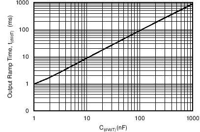
- 10.2.1.2.5 Setting Output Voltage Ramp time (tdVdT)
- 10.2.1.2.6 Programing the Power Good Set Point
- 10.2.1.2.7 Support Component Selections - R6, R7 and CIN
- 10.2.1.3 Application Curves
- 10.2.1
eFuse for Enterprise SSDs
- 10.3 System Examples
- 11Power Supply Recommendations
- 12Layout
- 13器件和文档支持
- 14机械封装和可订购信息
7 Specifications
7.1 Absolute Maximum Ratings
over operating temperature range (unless otherwise noted) (1)| VALUE | UNIT | |||
|---|---|---|---|---|
| MIN | MAX | |||
| Input voltage range | IN, OUT, PGTH, PGOOD, EN/UVLO, OVP, DEVSLP, FLT | –0.3 | 20 | V |
| IN (10 ms Transient) | 22 | |||
| dVdT, ILIM | –0.3 | 3.6 | ||
| IMON | –0.3 | 7 | ||
| Sink current | PGOOD, FLT, dVdT | 10 | mA | |
| Source current | dVdT, ILIM, IMON | Internally Limited | ||
| Maximum junction, TJ | –40 | 150 | °C | |
| Continuous power dissipation | See the Thermal Characteristics | |||
(1) Stresses beyond those listed under absolute maximum ratings may cause permanent damage to the device. These are stress ratings only and functional operation of the device at these or any conditions beyond those indicated under recommended operating conditions is not implied. Exposure to absolute-maximum-rated conditions for extended periods may affect device reliability.
7.2 Handling Ratings
| MIN | MAX | UNIT | |||
|---|---|---|---|---|---|
| Tstg | Storage temperature range | –65 | 150 | °C | |
| VESD | Electrostatic discharge | Human body model (HBM), per ANSI/ESDA/JEDEC JS-001, all pins(1) | -2 | 2 | kV |
| Charged device model (CDM), per JEDEC specification JESD22-C101, all pins(2) | -500 | 500 | V | ||
(1) JEDEC document JEP155 states that 500-V HBM allows safe manufacturing with a standard ESD control process.
(2) JEDEC document JEP157 states that 250-V CDM allows safe manufacturing with a standard ESD control process.
7.3 Recommended Operating Conditions
over operating free-air temperature range (unless otherwise noted)| MIN | NOM | MAX | UNIT | ||
|---|---|---|---|---|---|
| Input voltage range | IN | 2.7 | 18 | V | |
| EN/UVLO, OVP, DEVSLP, OUT, PGTH, PGOOD, FLT | 0 | 18 | |||
| dVdT, ILIM | 0 | 3 | |||
| IMON | 0 | 6 | |||
| Resistance | ILIM | 16.9 | 150 | kΩ | |
| IMON | 1 | ||||
| External capacitance | OUT | 0.1 | µF | ||
| dVdT | 470 | nF | |||
| Operating junction temperature range, TJ | –40 | 25 | 125 | °C | |
7.4 Thermal Characteristics(1)
| THERMAL METRIC | TPS25940 | UNIT | |
|---|---|---|---|
| RVC (20) PINS | |||
| RθJA | Junction-to-ambient thermal resistance | 38.1 | °C/W |
| RθJCtop | Junction-to-case (top) thermal resistance | 40.5 | |
| RθJB | Junction-to-board thermal resistance | 13.6 | |
| ψJT | Junction-to-top characterization parameter | 0.6 | |
| ψJB | Junction-to-board characterization parameter | 13.7 | |
| RθJCbot | Junction-to-case (bottom) thermal resistance | 3.4 | |
(1) For more information about traditional and new thermal metrics, see the IC Package Thermal Metrics application report, SPRA953.
7.5 Electrical Characteristics
Conditions are –40°C ≤ TJ=TA ≤ 125°C, 2.7 V ≤ V(IN) = 18 V, V(EN/UVLO) = 2 V, V(OVP) = V(DEVSLP) = V(PGTH) = 0 V, R(ILIM) = 150 kΩ, C(OUT) = 1 µF, C(dVdT) = OPEN, PGOOD = FLT = IMON = OPEN. Positive current into terminals. All voltages referenced to GND (unless otherwise noted)| PARAMETER | TEST CONDITIONS | MIN | TYP | MAX | UNIT | |
|---|---|---|---|---|---|---|
| SUPPLY VOLTAGE AND INTERNAL UNDERVOLTAGE LOCKOUT | ||||||
| V(IN) | Operating Input Voltage | 2.7 | 18 | V | ||
| V(UVR) | Internal UVLO threshold, rising | 2.2 | 2.3 | 2.4 | V | |
| V(UVRhys) | Internal UVLO hysteresis | 105 | 116 | 125 | mV | |
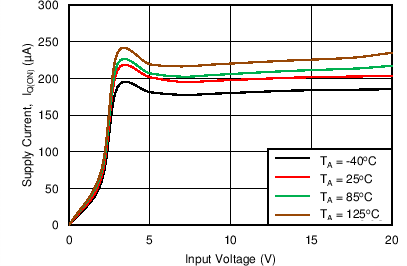
| IQ(ON) | Supply current, Enabled | V(EN/UVLO) = 2 V, V(IN) = 3 V | 140 | 210 | 300 | µA |
| V(EN/UVLO) = 2 V, V(IN) = 12 V | 140 | 199 | 260 | |||
| V(EN/UVLO) = 2 V, V(IN) = 18 V | 140 | 202 | 270 | |||
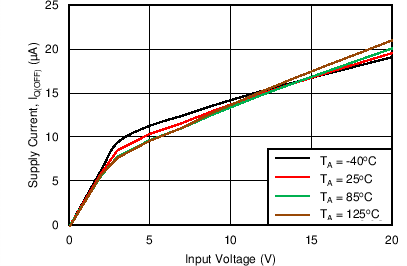
| IQ(OFF) | Supply current, Disabled | V(EN/UVLO) = 0 V, V(IN) = 3 V | 4 | 8.6 | 15 | µA |
| V(EN/UVLO) = 0 V, V(IN) = 12 V | 6 | 15 | 20 | |||
| V(EN/UVLO) = 0 V, V(IN) = 18 V | 8 | 18.5 | 25 | |||
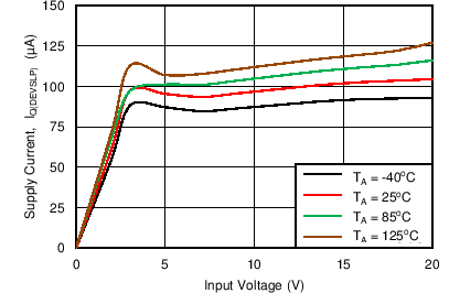
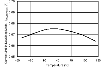
| IQ(DEVSLP) | Supply current, DevSleep Mode | V(DEVSLP) = 0 V, V(IN) = 2.7V to 18V | 70 | 95 | 130 | µA |
| ENABLE AND UNDERVOLTAGE LOCKOUT (EN/UVLO) INPUT | ||||||
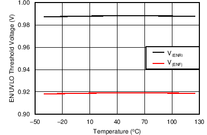
| V(ENR) | EN/UVLO threshold voltage, rising | 0.97 | 0.99 | 1.01 | V | |
| V(ENF) | EN/UVLO threshold voltage, falling | 0.9 | 0.92 | 0.94 | V | |
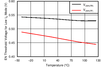
| V(SHUTF) | EN threshold voltage for Low IQ shutdown, falling | 0.3 | 0.47 | 0.63 | V | |
| V(SHUTFhys) | EN hysteresis for low IQ shutdown, hysteresis(1) | 66 | mV | |||
| IEN | EN Input leakage current | 0 V ≤ V(EN/UVLO) ≤ 18 V | –100 | 0 | 100 | nA |
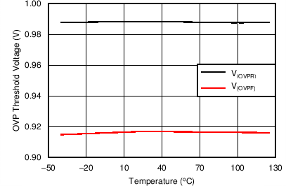
| OVER VOLTAGE PROTECTION (OVP) INPUT | ||||||
| V(OVPR) | Overvoltage Threshold Voltage, Rising, | 0.97 | 0.99 | 1.01 | V | |
| V(OVPF) | Overvoltage Threshold Voltage, Falling | 0.9 | 0.92 | 0.94 | V | |
| I(OVP) | OVP Input Leakage Current | 0 V ≤ V(OVP) ≤ 5 V | -100 | 0 | 100 | nA |
| DEVSLP MODE INPUT (DEVSLP): ACTIVE HIGH | ||||||
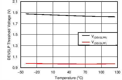
| V(DEVSLPR) | DEVSLP threshold voltage, rising | 1.6 | 1.85 | 2 | V | |
| V(DEVSLPF) | DEVSLP threshold voltage, falling | 0.8 | 0.96 | 1.1 | V | |
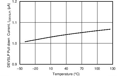
| I(DEVSLP) | DEVSLP input leakage current | 0.2 V ≤ V(DEVSLP) ≤ 18 V | 0.6 | 1 | 1.25 | µA |
| OUTPUT RAMP CONTROL (dVdT) | ||||||
| I(dVdT) | dVdT charging current | V(dVdT) = 0 V | 0.85 | 1 | 1.15 | µA |
| R(dVdT) | dVdT discharging resistance | EN/UVLO = 0 V, I(dVdT) = 10 mA sinking | 16 | 24 | Ω | |
| V(dVdTmax) | dVdT maximum capacitor voltage | 2.6 | 2.88 | 3.1 | V | |
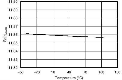
| GAIN(dVdT) | dVdT to OUT gain | ΔV(OUT)/ΔV(dVdT) | 11.65 | 11.9 | 12.05 | V/V |
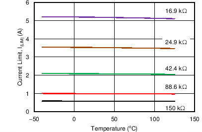
| CURRENT LIMIT PROGRAMMING (ILIM) | ||||||
| V(ILIM) | ILIM bias voltage | 0.87 | V | |||
| I(LIM) | Current limit(2) | R(ILIM) = 150 kΩ, (V(IN) - V(OUT)) = 1 V | 0.53 | 0.58 | 0.63 | A |
| R(ILIM) = 88.7 kΩ, (V(IN) - V(OUT)) = 1 V | 0.9 | 0.99 | 1.07 | |||
| R(ILIM) = 42.2 kΩ, (V(IN) - V(OUT)) = 1 V | 1.92 | 2.08 | 2.25 | |||
| R(ILIM) = 24.9 kΩ, (V(IN) - V(OUT)) = 1 V | 3.25 | 3.53 | 3.81 | |||
| R(ILIM) = 16.9 kΩ, (V(IN) - V(OUT)) = 1 V | 4.78 | 5.2 | 5.62 | |||
| R(ILIM) = OPEN, Open resistor current limit (Single Point Failure Test: UL60950) | 0.35 | 0.45 | 0.55 | |||
| R(ILIM) = SHORT, Shorted resistor current limit (Single Point Failure Test: UL60950) | 0.55 | 0.67 | 0.8 | |||
| I(DEVSLP(LIM)) | DevSleep Mode Current Limit | 0.55 | 0.67 | 0.8 | A | |
| IOS | Short-circuit current limit (2) | R(ILIM) = 42.2 kΩ, V(VIN) = 12 V, (V(IN) -V(OUT)) = 5 V | 1.91 | 2.07 | 2.24 | A |
| R(ILIM) = 24.9 kΩ, V(VIN) = 12 V, (V(IN) -V(OUT)) = 5 V | 3.21 | 3.49 | 3.77 | |||
| R(ILIM) = 16.9 kΩ, V(VIN) = 12 V, (V(IN) -V(OUT))= 5 V, -40°C ≤ TJ ≤ 85°C | 4.7 | 5.11 | 5.52 | |||
| I(FASTRIP) | Fast-Trip comparator threshold(1)(2) | 1.5 x I(LIM) + 0.375 | A | |||
| CURRENT MONITOR OUTPUT (IMON) | ||||||
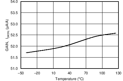
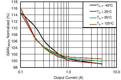
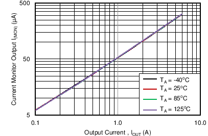
| GAIN(IMON) | Gain Factor I(IMON):I(OUT) | 1 A ≤ I(OUT) ≤ 5 A | 47.78 | 52.3 | 57.23 | µA/A |
| MOSFET – POWER SWITCH | ||||||
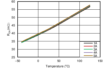
| RON | IN to OUT - ON Resistance | 1 A ≤ I(OUT) ≤ 5 A, TJ = 25°C | 34 | 42 | 49 | mΩ |
| 1 A ≤ I(OUT) ≤ 5 A, -40°C ≤ TJ ≤ 85°C | 26 | 42 | 58 | |||
| 1 A ≤ I(OUT) ≤ 5 A, -40°C ≤ TJ ≤ 125°C | 26 | 42 | 64 | |||
| PASS FET OUTPUT (OUT) | ||||||
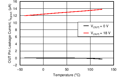
| Ilkg(OUT) | OUT leakage current in off state | V(IN) = 18 V, V(EN/UVLO) = 0 V, V(OUT) = 0 V (Sourcing) | –2 | 0 | 2 | µA |
| V(IN) = 2.7 V, V(EN/UVLO) = 0 V, V(OUT) = 18 V (Sinking) | 6 | 13 | 20 | |||
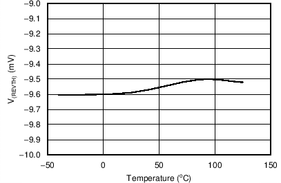
| V(REVTH) | V(IN) -V(OUT) threshold for reverse protection comparator, falling | –15 | -9.3 | –3 | mV | |
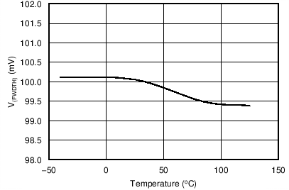
| V(FWDTH) | V(IN) -V(OUT) threshold for reverse protection comparator, rising | 86 | 100 | 114 | mV | |
| FAULT FLAG (FLT): ACTIVE LOW | ||||||
| R(FLT) | FLT internal pull-down resistance | V(OVP) = 2 V, I(FLT) = 5 mA sinking | 10 | 18 | 30 | Ω |
| I(FLT) | FLT input leakage current | 0 V ≤ V(FLT) ≤ 18 V | –1 | 0 | 1 | µA |
| POSITIVE INPUT for POWER-GOOD COMPARATOR (PGTH) | ||||||
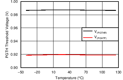
| V(PGTHR) | PGTH threshold voltage, rising | 0.97 | 0.99 | 1.01 | V | |
| V(PGTHF) | PGTH threshold voltage, falling | 0.9 | 0.92 | 0.94 | V | |
| I(PGTH) | PGTH input leakage current | 0 V ≤ V(PGTH) ≤ 18 V | –100 | 0 | 100 | nA |
| POWER-GOOD COMPARATOR OUTPUT (PGOOD): ACTIVE HIGH | ||||||
| R(PGOOD) | PGOOD internal pull-down resistance | V(PGTH) = 0V, I(PGOOD) = 5 mA sinking | 10 | 20 | 35 | Ω |
| I(PGOOD) | PGOOD input leakage current | 0 V ≤ V(PGOOD) ≤ 18 V | –1 | 0 | 1 | µA |
| THERMAL SHUT DOWN (TSD) | ||||||
| T(TSD) | TSD Threshold(1) | 160 | °C | |||
| T(TSDhys) | TSD Hysteresis(1) | 12 | °C | |||
| Thermal Fault: (Latched or Auto-Retry) | TPS25940L | LATCHED | ||||
| TPS25940A | AUTO-RETRY | |||||
(1) These parameters are provided for reference only and do not constitute part of TI's published device specifications for purposes of TI's product warranty.
(2) Pulse-testing techniques maintain junction temperature close to ambient temperature. Thermal effects must be taken into account separately.
7.6 Timing Requirements
Conditions are –40°C ≤ TJ=TA ≤ 125°C, 2.7 V ≤ V(IN) = 18 V, V(EN/UVLO) = 2 V, V(OVP) = V(DEVSLP) = V(PGTH) = 0 V, R(ILIM) = 150 kΩ, C(OUT) = 1 µF, C(dVdT) = OPEN, PGOOD = FLT = IMON = OPEN. Positive current into terminals. All voltages referenced to GND (unless otherwise noted). Refer to Figure 42 for the timing diagrams.| PARAMETER | TEST CONDITIONS | MIN | TYP | MAX | UNIT | |
|---|---|---|---|---|---|---|
| ENABLE and UVLO INPUT | ||||||
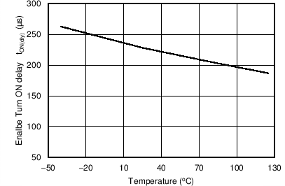
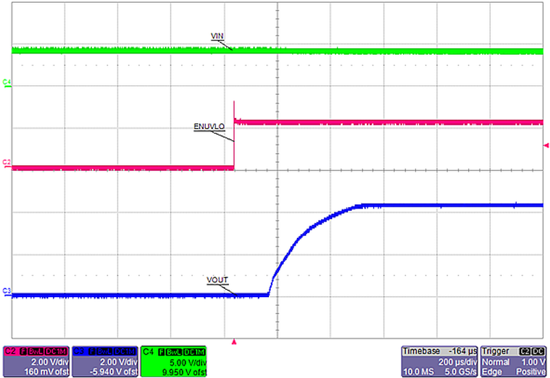
| tON(dly) | EN turn on delay | EN/UVLO ↑ (100mV above V(ENR)) to V(OUT) = 100 mV, C(dVdT) < 0.8 nF |
220 | µs | ||
| EN/UVLO ↑ (100mV above V(ENR)) to V(OUT) = 100 mV, C(dVdT) ≥ 0.8 nF, [C(dVdT) in nF] |
100 + 150 x C(dVdT) | µs | ||||
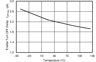
| tOFF(dly) | EN turn off delay | EN/UVLO ↓ (100mV below V(ENF)) to FLT↓ | 2 | µs | ||
| OVERVOLTAGE PROTECTION INPUT (OVP) | ||||||
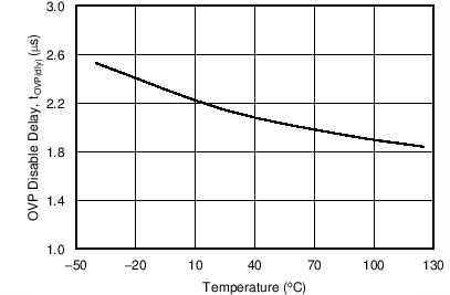
| tOVP(dly) | OVP disable delay | OVP↑ (100mV above V(OVPR)) to FLT↓ | 2 | µs | ||
| OUTPUT RAMP CONTROL (dV/dT ) | ||||||
| tdVdT | Output ramp time | EN/UVLO ↑ to V(OUT) = 4.5 V, with C(dVdT) = open | 0.12 | ms | ||
| EN/UVLO ↑ to V(OUT) = 11 V, with C(dVdT) = open | 0.25 | 0.37 | 0.5 | |||
| EN/UVLO ↑ to V(OUT) = 11 V, with C(dVdT) = 1 nF | 0.97 | |||||
| CURRENT LIMIT | ||||||
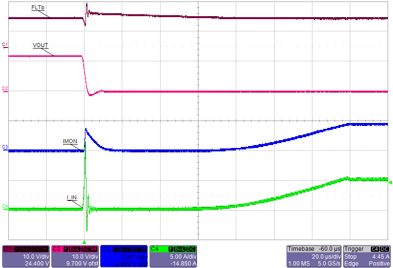
| tFASTRIP(dly) | Fast-Trip comparator delay | I(OUT) > I(FASTRIP) | 200 | ns | ||
| REVERSE PROTECTION COMPARATOR | ||||||
| tREV(dly) | Reverse protection comparator delay | (V(IN) - V(OUT))↓ (1 mV overdrive below V(REVTH)) to FLT↓ | 10 | µs | ||
| (V(IN) - V(OUT))↓ (10 mV overdrive below V(REVTH)) to FLT↓ | 1 | |||||
| tFWD(dly) | (V(IN) - V(OUT))↑ (10 mV overdrive above V(FWDTH)) to FLT↑ | 3.1 | ||||
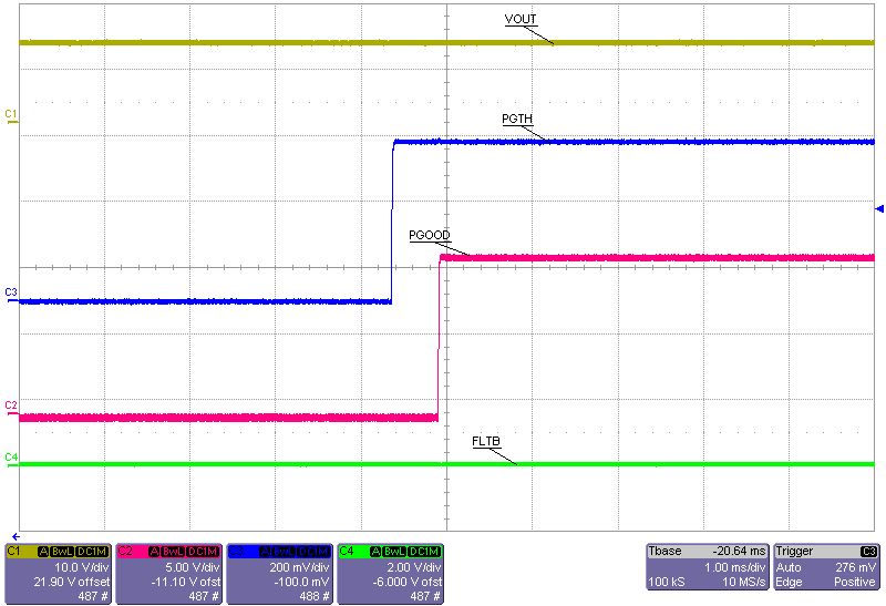
| POWER-GOOD COMPARATOR OUTPUT (PGOOD): ACTIVE HIGH | ||||||
| tPGOODR | PGOOD delay (de-glitch) time | Rising edge | 0.42 | 0.54 | 0.66 | ms |
| tPGOODF | Falling edge | 0.42 | 0.54 | 0.66 | ms | |
| THERMAL SHUT DOWN (TSD) | ||||||
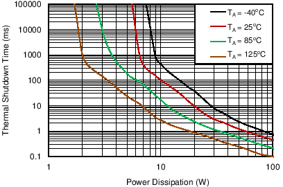
| Retry delay in TSD | TPS25940A Only | 128 | ms | |||
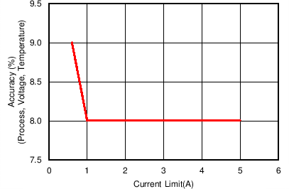
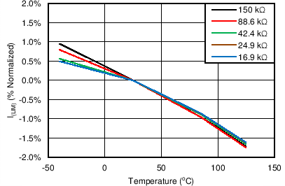
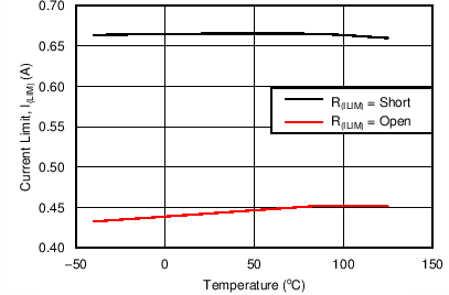
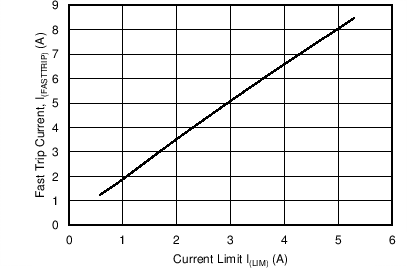
7.7 Typical Characteristics
Conditions are –40°C ≤ TA = TJ ≤ 125°C, V(IN) = 12 V, V(EN/UVLO) = 2 V, V(OVP) = V(DEVSLP) = V(PGTH) = 0 V, R(ILIM) = 150 kΩ, C(OUT) = 1 µF, C(dVdT) = OPEN, PGOOD = FLT = IMON = OPEN. (unless stated otherwise)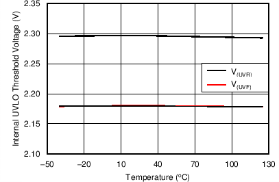
| Taken on 2-Layer board, 2oz.(0.08-mm thick) with GND plane area: 14 cm2 (Top) and 20 cm2 (bottom) |
| V(IN) = 11 V |
.png)
| R(FLT)=100 kΩ |
.png)
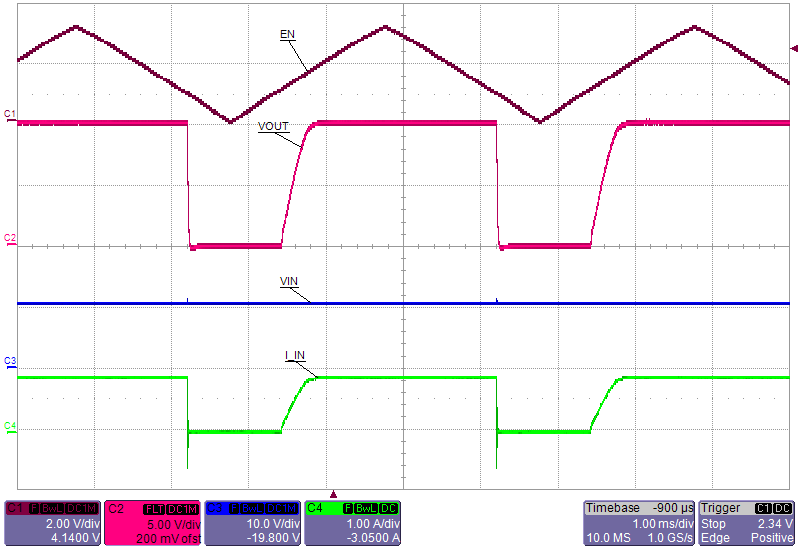
| V(IN) = 12 V | RL = 12 Ω | R(FLT)=100 kΩ |
| V(IN) = 12 V | RL = 12 Ω | R(FLT)= 100 kΩ |
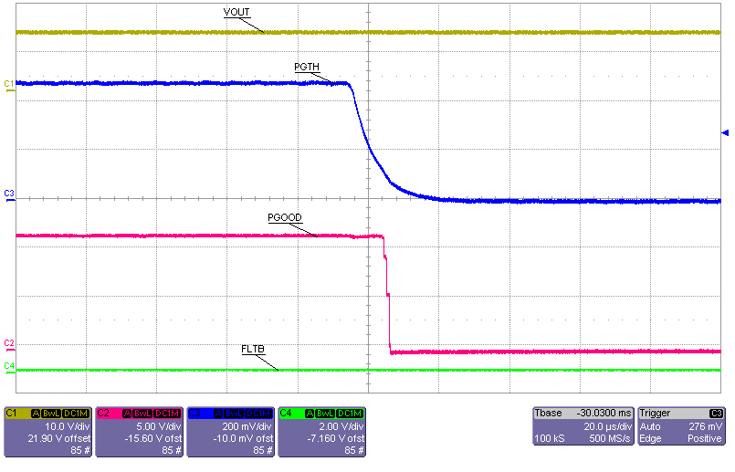
| R(PGOOD)= 100 kΩ |
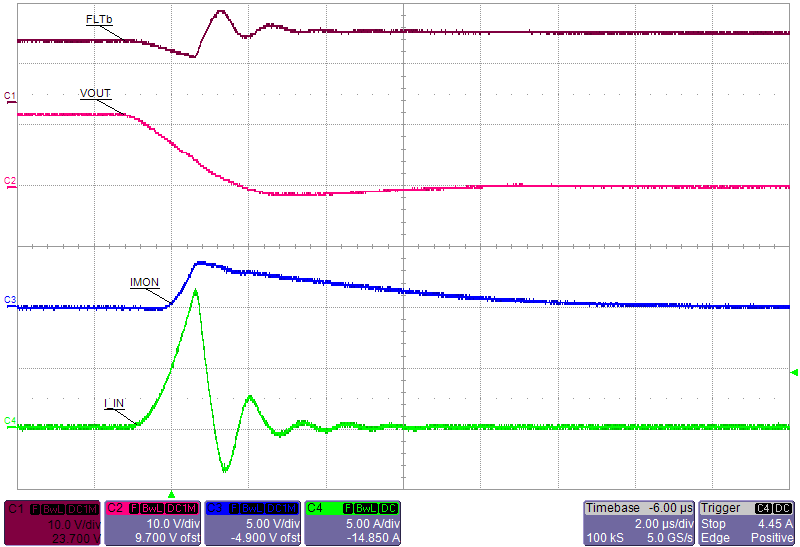
| R(FLT)=100 kΩ | R(IMON)= 16.9 kΩ |

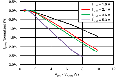
| Thermal shutdown occurs when I(LIM) = 5.3 A | ||
| and [V(IN) - V(OUT)] > 8 V | ||
| V(IN) = 4.5 V | ||
.png)
| R(FLT)=100 kΩ |
.png)
| V(IN) = 12 V | RL = 12 Ω | R(FLT)=100 kΩ |
| V(IN) = 12 V | RL = 12 Ω | R(FLT)= 100 kΩ |
| R(PGOOD)= 100 kΩ |
| R(FLT) =100 kΩ | R(IMON)= 16.9 kΩ | |