ZHCSCK2 June 2014
PRODUCTION DATA.
- 1 特性
- 2 应用范围
- 3 说明
- 4 简化电路原理图
- 5 修订历史记录
- 6 Pin Configuration and Functions
- 7 Specifications
- 8 Parametric Measurement Information
-
9 Detailed Description
- 9.1 Overview
- 9.2 Functional Block Diagram
- 9.3
Feature Description
- 9.3.1 Enable and Adjusting Undervoltage Lockout
- 9.3.2 Overvoltage Protection (OVP)
- 9.3.3 Hot Plug-in and In-Rush Current Control
- 9.3.4 Overload and Short Circuit Protection :
- 9.3.5 FAULT Response
- 9.3.6 Current Monitoring:
- 9.3.7 Power Good Comparator
- 9.3.8 IN, OUT and GND Pins
- 9.3.9 Thermal Shutdown:
- 9.4 Device Functional Modes
-
10Application and Implementation
- 10.1 Application Information
- 10.2
Typical Application
- 10.2.1
eFuse for Enterprise SSDs
- 10.2.1.1 Design Requirements
- 10.2.1.2
Detailed Design Procedure
- 10.2.1.2.1 Step by Step Design Procedure
- 10.2.1.2.2 Programming the Current-Limit Threshold: R(ILIM) Selection
- 10.2.1.2.3 Undervoltage Lockout and Overvoltage Set Point
- 10.2.1.2.4 Programming Current Monitoring Resistor - RIMON
- 10.2.1.2.5 Setting Output Voltage Ramp time (tdVdT)
- 10.2.1.2.6 Programing the Power Good Set Point
- 10.2.1.2.7 Support Component Selections - R6, R7 and CIN
- 10.2.1.3 Application Curves
- 10.2.1
eFuse for Enterprise SSDs
- 10.3 System Examples
- 11Power Supply Recommendations
- 12Layout
- 13器件和文档支持
- 14机械封装和可订购信息
10 Application and Implementation
10.1 Application Information
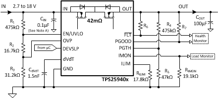
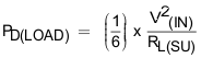
The TPS25940 is a smart eFuse. It is typically used for Hot-Swap and Power rail protection applications. It operates from 2.7 V to 18 V with programmable current limit, overvoltage and undervoltage protection. The device aids in controlling the in-rush current and provides fast turn-off during reverse voltage conditions for systems such as Enterprise SSDs, HDDs, Servers, Power Back-up Storage units and RAID cards. The device also provides robust protection for multiple faults on the sub-system rail.
The following design procedure can be used to select component values for the device.
Alternatively, the WEBENCH® software may be used to generate a complete design. The WEBENCH® software uses an iterative design procedure and accesses a comprehensive database of components when generating a design. Additionally, a spreadsheet design tool TPS25940 Design Calculator is available on web folder.
This section presents a simplified discussion of the design process.
10.2 Typical Application
10.2.1 eFuse for Enterprise SSDs
10.2.1.1 Design Requirements
Table 1. Design Parameters
| DESIGN PARAMETER | EXAMPLE VALUE |
|---|---|
| Input voltage range, V(IN) | 12 V |
| Undervoltage lockout set point, V(UV) | 10.8 V |
| Overvoltage protection set point , V(LIM) | 16.5 V |
| Load at Start-Up , RL(SU) | 4.8 Ω |
| Current limit, I(LIM) | 5 A |
| Load capacitance , C(OUT) | 100 µF |
| Maximum ambient temperatures , TA | 85°C |
10.2.1.2 Detailed Design Procedure
The following design procedure can be used to select component values for the TPS25940A and TPS25940L.
10.2.1.2.1 Step by Step Design Procedure
To begin the design process a few parameters must be decided upon. The designer needs to know the following:
- Normal input operation voltage
- Maximum output capacitance
- Maximum current Limit
- Load during start-up
- Maximum ambient temperature of operation
This design procedure below seeks to control the junction temperature of device under both static and transient conditions by proper selection of output ramp-up time and associated support components. The designer can adjust this procedure to fit the application and design criteria.
10.2.1.2.2 Programming the Current-Limit Threshold: R(ILIM) Selection
The R(ILIM) resistor at the ILIM pin sets the over load current limit, this can be set using Equation 4.
Choose closest standard value: 17.8k, 1% standard value resistor.
10.2.1.2.3 Undervoltage Lockout and Overvoltage Set Point
The undervoltage lockout (UVLO) and overvoltage trip point are adjusted using the external voltage divider network of R1, R2 and R3 as connected between IN, EN, OVP and GND pins of the device. The values required for setting the undervoltage and overvoltage are calculated solving Equation 10 and Equation 11.
For minimizing the input current drawn from the power supply {I(R123) = V(IN)/(R1 + R2 + R3)}, it is recommended to use higher values of resistance for R1, R2 and R3.
However, leakage currents due to external active components connected to the resistor string can add error to these calculations. So, the resistor string current, I(R123) must be chosen to be 20x greater than the leakage current expected.
From the device electrical specifications, V(OVPR) = 0.99 V and V(ENR) = 0.99 V. For design requirements, V(OV) is 16.5 V and V(UV) is 10.8 V. To solve the equation, first choose the value of R3 = 31.2 kΩ and use Equation 10 to solve for (R1 + R2) = 488.8 kΩ. Use Equation 11 and value of (R1 + R2) to solve for R2 = 16.47 kΩ and finally R1= 472.33 kΩ.
Using the closest standard 1% resistor values gives R1 = 475 kΩ, R2 = 16.7 kΩ, and R3 = 31.2 kΩ.
The power failure threshold is detected on the falling edge of supply. This threshold voltage is 7% lower than the rising threshold, V(UV). This is calculated using Equation 12.
10.2.1.2.4 Programming Current Monitoring Resistor - RIMON
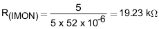
Voltage at IMON pin V(IMON) represents the voltage proportional to load current. This can be connected to an ADC of the downstream system for health monitoring of the system. The R(IMON) need to be configured based on the maximum input voltage range of the ADC used. R(IMON) is set using Equation 13.
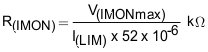
For I(LIM) = 5 A, and considering the operating range of ADC from 0 V to 5 V, V(IMONmax) is 5 V and R(IMON) is determined by:
Selecting R(IMON) value less than determined by Equation 14 ensures that ADC limits are not exceeded for maximum value of load current.
If the IMON pin voltage is not being digitized with an ADC, R(IMON) can be selected to produce a 1V/1A voltage at the IMON pin, using Equation 13.
Choose closest 1 % standard value: 19.1 kΩ.
If current monitoring up to I(FASTRIP) is desired, R(IMON) can be reduced by a factor of 1.6, as in Equation 5.
10.2.1.2.5 Setting Output Voltage Ramp time (tdVdT)
For a successful design, the junction temperature of device should be kept below the absolute-maximum rating during both dynamic (start-up) and steady state conditions. Dynamic power stresses often are an order of magnitude greater than the static stresses, so it is important to determine the right start-up time and in-rush current limit required with system capacitance to avoid thermal shutdown during start-up with and without load.
The ramp-up capacitor C(dVdT) needed is calculated considering the two possible cases:
10.2.1.2.5.1 Case1: Start-up Without Load: Only Output Capacitance C(OUT) Draws Current During Start-up
During start-up, as the output capacitor charges, the voltage difference across the internal FET decreases, and the power dissipated decreases as well. Typical ramp-up of output voltage V(OUT) with inrush current limit of 1.2A and power dissipated in the device during start-up is shown in Figure 53. The average power dissipated in the device during start-up is equal to area of triangular plot (red curve in Figure 54) averaged over tdVdT.
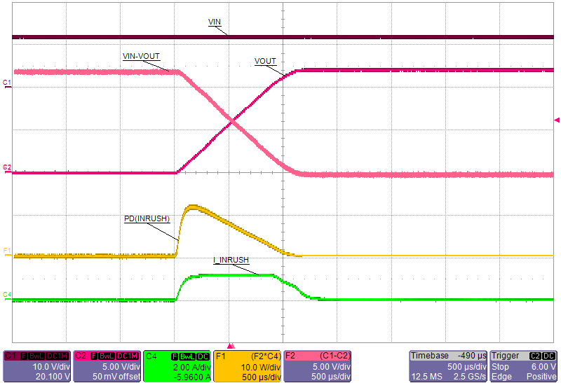
| V(IN) = 12 V | C(dVdT) = 1 nF | C(OUT)=100 µF |
| V(IN) = 12 V | C(dVdT) = 1 nF | C(OUT)=100 µF |
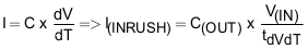
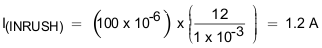
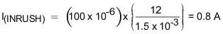
For TPS25940 device, the inrush current is determined as,
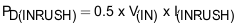
Power dissipation during start-up is:
Equation 16 assumes that load does not draw any current until the output voltage has reached its final value.
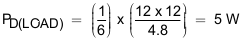
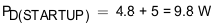
10.2.1.2.5.2 Case 2: Start-up With Load: Output Capacitance C(OUT) and Load Draws Current During Start-up
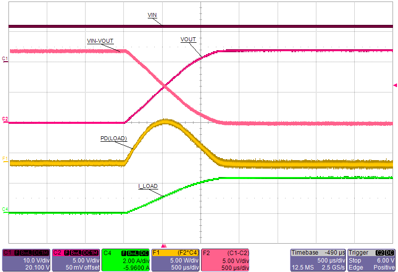
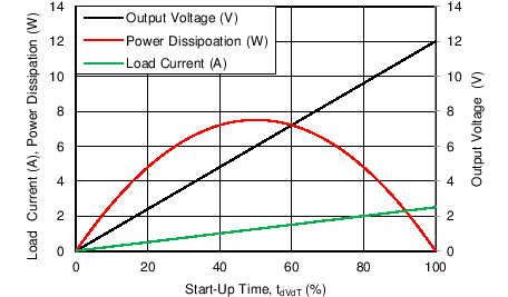
When load draws current during the turn-on sequence, there will be additional power dissipated. Considering a resistive load RL(SU) during start-up, load current ramps up proportionally with increase in output voltage during tdVdT time. Typical ramp-up of output voltage, Load current and power dissipation in the device is shown in Figure 55 and power dissipation with respect to time is plotted in Figure 56. The additional power dissipation during start-up phase is calculated as follows.
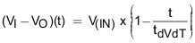
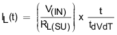
Where RL(SU) is the load resistance present during start-up. Average energy loss in the internal FET during charging time due to resistive load is given by:
| V(IN) = 12 V | C(dVdT) = 1 nF | RL(SU) = 4.8 Ω |
| V(IN) = 12 V | C(dVdT) = 1 nF | RL(SU) = 4.8 Ω |
On solving Equation 19 the average power loss in the internal FET due to load is:
Total power dissipated in the device during startup is:

Total current during startup is given by:
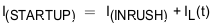
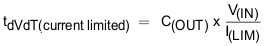
If I(STARTUP) > I(LIM), the device limits the current to I(LIM) and the current limited charging time is determined by:
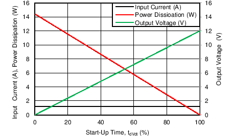
The power dissipation, with and without load, for selected start-up time should not exceed the shutdown limits as shown in Figure 57.
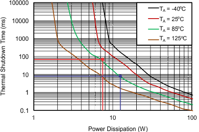 Figure 57. Thermal Shutdown Limit Plot
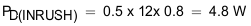
For the design example under discussion,
Select ramp-up capacitor C(dVdT) = 1nF, using Equation 2.

The inrush current drawn by the load capacitance (C(OUT)) during ramp-up using Equation 3.
The inrush Power dissipation is calculated, using Equation 16.
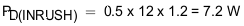
For 7.2 W of power loss, the thermal shut down time of the device should not be less than the ramp-up time tdVdT to avoid the false trip at maximum operating temperature. From thermal shutdown limit graph Figure 57 at TA = 85°C, for 7.2 W of power the shutdown time is ~60 ms. So it is safe to use 1 ms as start-up time without any load on output.
Considering the start-up with load 4.8 Ω, the additional power dissipation, when load is present during start up is calculated, using Equation 20.
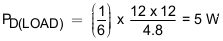
The total device power dissipation during start up is:
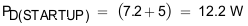
From thermal shutdown limit graph at TA = 85°C, the thermal shutdown time for 12.2 W is close to 7.5 ms. It is safe to have 30% margin to allow for variation of system parameters such as load, component tolerance, and input voltage. So it is well within acceptable limits to use the 1 nF capacitor with start-up load of 4.8 Ω.
If there is a need to decrease the power loss during start-up, it can be done with increase of C(dVdT) capacitor.
To illustrate, choose C(dVdT) = 1.5 nF as an option and recalculate:

From thermal shutdown limit graph at TA = 85°C, the shutdown time for 10 W power dissipation is ~17 ms, which increases the margins further for shutdown time and ensures successful operation during start up and steady state conditions.
The spreadsheet tool available on the web can be used for iterative calculations.
10.2.1.2.6 Programing the Power Good Set Point
As shown in Figure 52, R4 and R5 sets the required limit for PGOOD signal as needed for the downstream converters. Considering a power good threshold of 11 V for this design, the values of R4 and R5 are calculated using Equation 34.
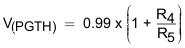
It is recommended to have high values for these resistors to limit the current drawn from the output node. Choosing a value of R4 = 475 kΩ, R5 = 47 kΩ provides V(PGTH) = 11 V.
10.2.1.2.7 Support Component Selections - R6, R7 and CIN
Reference to application schematics, R6 and R7 are required only if PGOOD and FLT are used; these resistors serve as pull-ups for the open-drain output drivers. The current sunk by each of these pins should not exceed 10 mA (refer to the Absolute Maximum Ratings table). CIN is a bypass capacitor to help control transient voltages, unit emissions, and local supply noise. Where acceptable, a value in the range of 0.001 μF to 0.1 μF is recommended for C(IN).
10.2.1.3 Application Curves
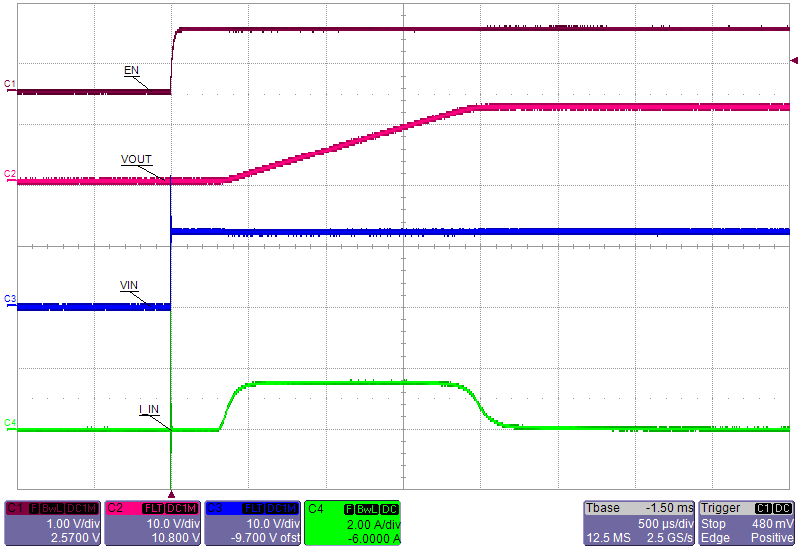 Figure 58. Hot-Plug Start-Up: Output Ramp Without Load on output
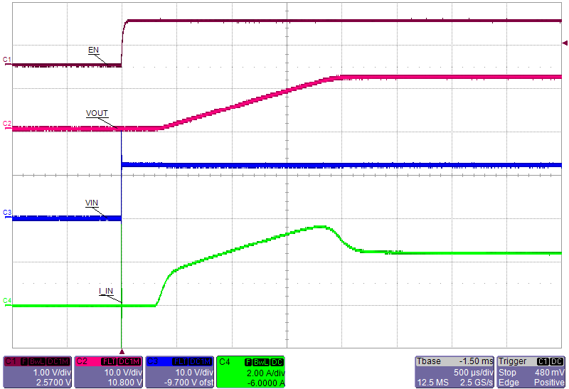 Figure 59. Hot-Plug Start-Up: Output Ramp With Start-up load of 4.8Ω
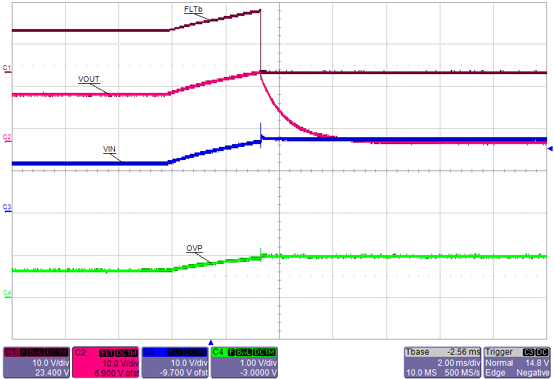 Figure 60. Overvoltage Shutdown
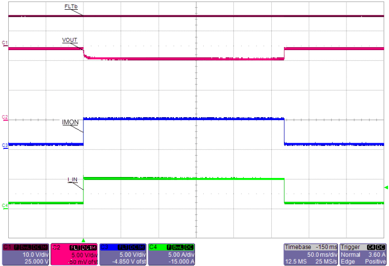 Figure 62. Over Load: Step Change in Load from 12Ω to 2Ω and Back
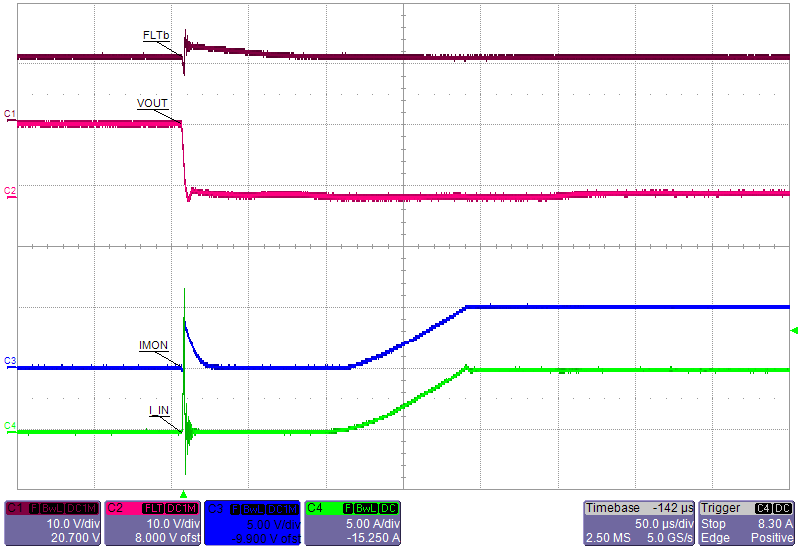 Figure 64. Hot Short: Fast Trip and Current Regulation
 Figure 66. Hot Short: Auto-Retry and Recovery from Short Circuit - TPS25940A
 Figure 68. Hot Plug-in with Short on Output: Auto-Retry - TPS25940A
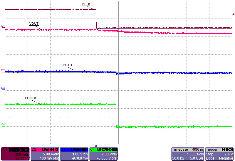 Figure 70. Power Good Response During Turn-OFF
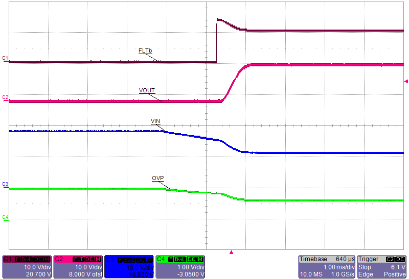 Figure 61. Overvoltage Recovery
 Figure 63. Overload Condition: Auto Retry and Recovery - TPS25940A
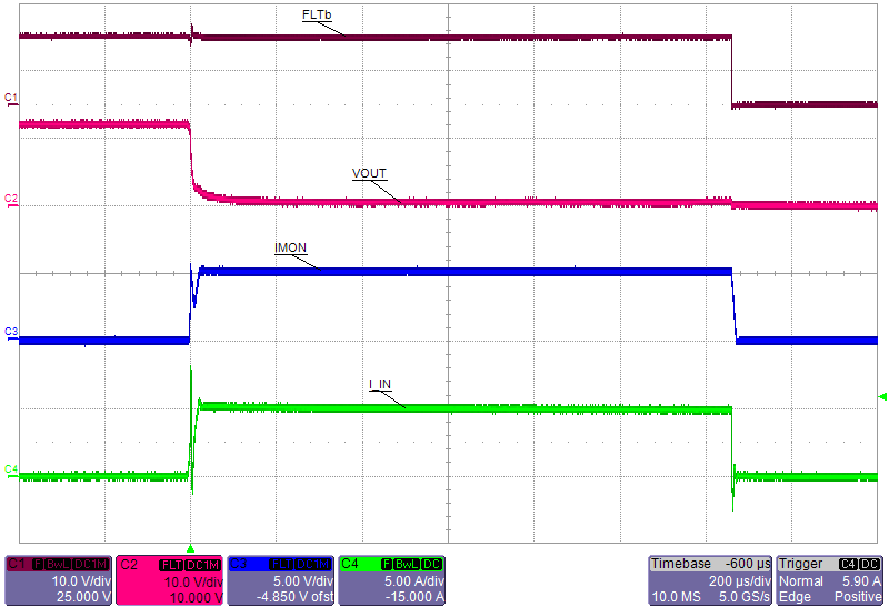 Figure 65. Hot Short: Latched - TPS25940L
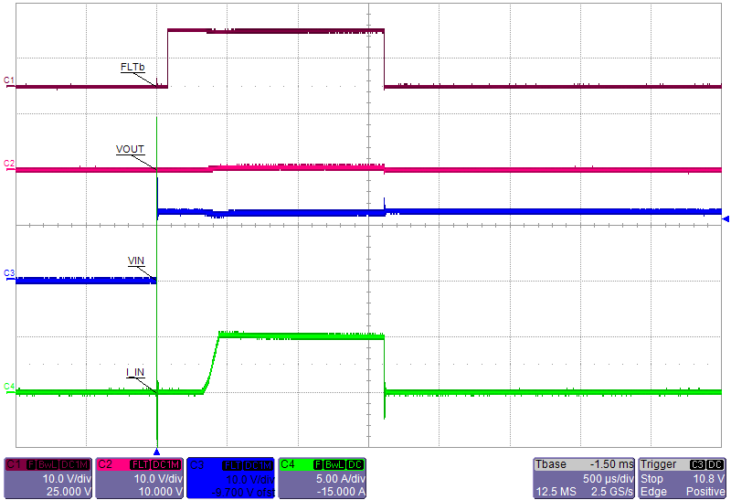 Figure 67. Hot Plug-in with Short on Output: Latched - TPS25940L
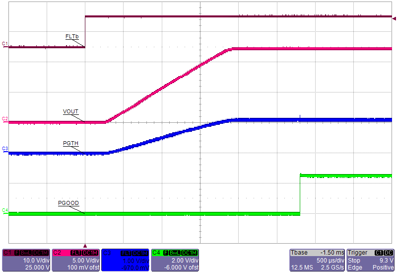 Figure 69. Power Good Response During Turn-ON
10.3 System Examples
10.3.1 Power Failure Protection and Data Retention in SSDs
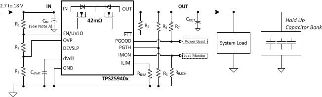
For enterprise and Industrial SSDs, it is necessary to have hold-up circuit and capacitor bank to ensure that critical user data is never lost during power-failure to the drive. The power-failure event could be due to momentary loss of power regulation (transient brown-out condition) or due to loss of power when drive is hot-plugged out.
The TPS25940 continuously monitors the supply voltage at EN/UVLO pin and swiftly disconnects the input bus from output when the voltage drops below a predefined threshold (power fail detection). The TPS25940 also monitors the reverse voltage from IN to OUT and when it exceeds -10 mV, it stops the flow of reverse current. In addition, it provides an instant warning signal (FLT) to the SSD controller to initiate the data hardening process. Its swift true reverse blocking feature reacts in 1 µs (typical) ensuring that the capacitor bank charge is retained. This helps the drive to have power for longer time to harden data and reduces the capacitance required in the hold-up bank, saving system cost.
The typical application diagram and application schematic of TPS25940 usage for enterprise SSD are shown in Figure 71 and Figure 72
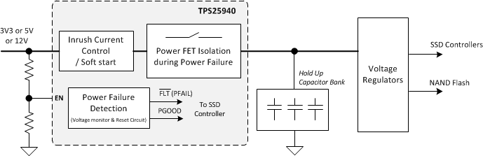 Figure 71. Power Circuit Block Diagram of Enterprise and Industrial SSDs
The oscilloscope plots demonstrating the true reverse blocking, fast turn-off and FLT signal delay are shown in Figure 73 through Figure 75.
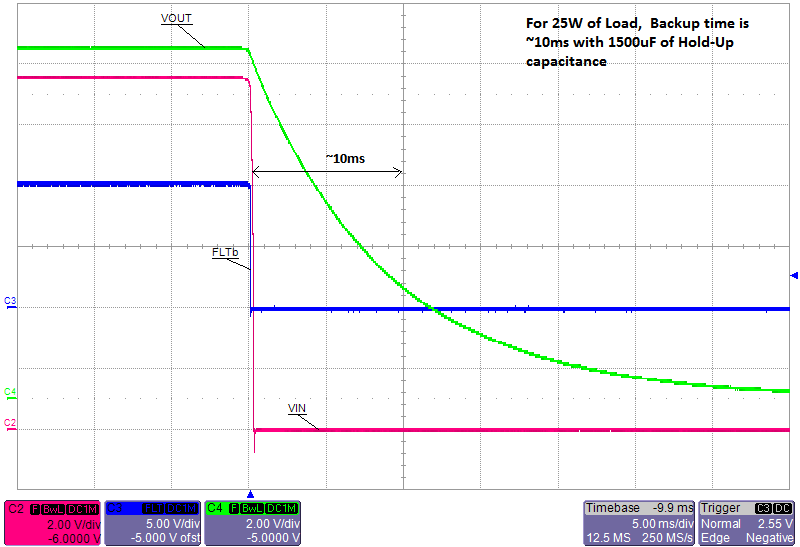
| V(IN) = 12V | C(OUT) = 1500 µF | RL = 5.6 Ω |
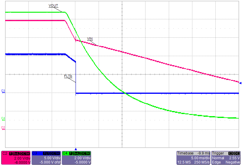
| V(IN) = 12V | C(OUT) = 1500 µF | RL = 5.6 Ω |
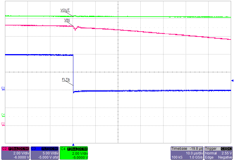
| V(IN) = 12V | C(OUT) = 1500 µF | RL = 5.6 Ω |
10.3.2 Boost Power Rail Configuration for Data Retention in Enterprise SSDs
In certain enterprise SSD architectures, the hold-up capacitor voltage is boosted to value higher than the input bus voltage to optimize the storage capacitor bank. A typical boosted hold-up voltage ranges from 12 V to 18 V. A typical power circuit block diagram is shown in Figure 76. For these applications, TPS25940 provides quick and smooth changeover of the power from main input bus to boosted backup voltage.
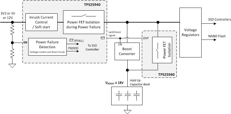 Figure 76. Power Circuit Block Diagram with Boosted Backup Power for Enterprise SSD
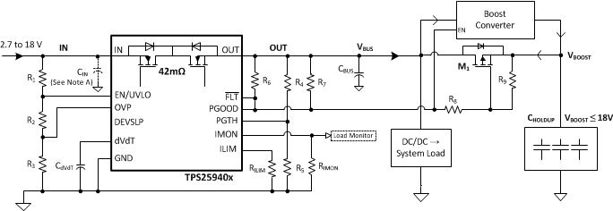
A typical application schematic for implementation of boosted backup power configuration is shown in Figure 77. During startup TPS25940 provides the inrush current control to charge up the C(BUS) as well as C(HOLDUP) close to V(IN). Once V(BUS) reaches the programmed PGOOD threshold, the boost converter is enabled to charge C(HOLDUP) to V(BOOST). When V(IN) fails, TPS25940 detects power failure and asserts the fault signal (FLT), which in turn disables the boost converter and shorts V(BOOST) to V(BUS), through M1. The FLT signal can be interfaced to SSD controller to initiate the data hardening process. If current limit protection is desired during data hardening process (when holdup capacitor is supplying system bus), M1 can be replaced by another TPS25940.
The oscilloscope plot demonstrating change over from Main (12 V) to Boosted backup power (14.5 V) is shown in Figure 78.
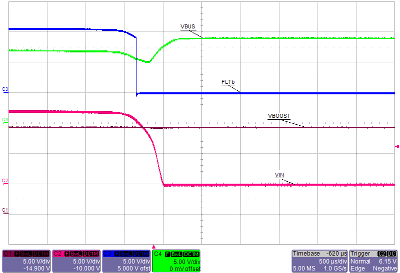
| V(IN) = 12 V | V(BOOST) = 14.5 V | C(BUS) = 150 µF | |
| P(LOAD) = 12.5 W | V(IN-UVLO-low) = 10.2 V | C(dVdT) = 1 nF |