ZHCSCK2 June 2014
PRODUCTION DATA.
- 1 特性
- 2 应用范围
- 3 说明
- 4 简化电路原理图
- 5 修订历史记录
- 6 Pin Configuration and Functions
- 7 Specifications
- 8 Parametric Measurement Information
-
9 Detailed Description
- 9.1 Overview
- 9.2 Functional Block Diagram
- 9.3
Feature Description
- 9.3.1 Enable and Adjusting Undervoltage Lockout
- 9.3.2 Overvoltage Protection (OVP)
- 9.3.3 Hot Plug-in and In-Rush Current Control
- 9.3.4 Overload and Short Circuit Protection :
- 9.3.5 FAULT Response
- 9.3.6 Current Monitoring:
- 9.3.7 Power Good Comparator
- 9.3.8 IN, OUT and GND Pins
- 9.3.9 Thermal Shutdown:
- 9.4 Device Functional Modes
-
10Application and Implementation
- 10.1 Application Information
- 10.2
Typical Application
- 10.2.1
eFuse for Enterprise SSDs
- 10.2.1.1 Design Requirements
- 10.2.1.2
Detailed Design Procedure
- 10.2.1.2.1 Step by Step Design Procedure
- 10.2.1.2.2 Programming the Current-Limit Threshold: R(ILIM) Selection
- 10.2.1.2.3 Undervoltage Lockout and Overvoltage Set Point
- 10.2.1.2.4 Programming Current Monitoring Resistor - RIMON
- 10.2.1.2.5 Setting Output Voltage Ramp time (tdVdT)
- 10.2.1.2.6 Programing the Power Good Set Point
- 10.2.1.2.7 Support Component Selections - R6, R7 and CIN
- 10.2.1.3 Application Curves
- 10.2.1
eFuse for Enterprise SSDs
- 10.3 System Examples
- 11Power Supply Recommendations
- 12Layout
- 13器件和文档支持
- 14机械封装和可订购信息
1 特性
- 2.7V - 18V 工作电压,最大绝对值 20V
- 42mΩ RON(典型值)
- 0.6A 至 5.3A 可调电流限值 (±8%)
- IMON 电流指示器输出 (±8%)
- 200μA 工作 IQ(典型值)
- 95μA DevSleep 模式 IQ(典型值)
- 被禁用时,15µA IQ(典型值)
- ±2% 过压、欠压阈值
- 反向电流阻断
- 1µs 反向电压关闭
- 可编程 dVo/dt 控制
- 电源正常和故障输出
- -40°C 至 125°C 的结温范围
- UL2367 认证正在处理中
- UL60950 - 单点故障测试期间安全
2 应用范围
- PCIe/SATA/SAS 硬盘 (HDD) 和 SSD 硬盘
- 企业级和微型服务器
- 智能负载开关
- 机顶盒 (STB),数字电视 (DTV) 和游戏控制台
- RAID 卡 - 保持电源管理
- 电信交换机和路由器
- 适配器供电器件
3 说明
TPS25940 eFuse 电源开关是一款紧凑且特性丰富的电源管理器件,此器件具有一整套的保护功能,其中包括一个低功率 DevSleep™ 模式,此模式支持与 SATA™ 器件睡眠标准的兼容性。 宽工作范围可实现对很多常用直流总线电压的控制。 集成背靠背场效应晶体管 (FET) 提供双向电流控制,从而使得器件非常适合于那些具有负载侧保持能量,而这些能量又一定不能回流至故障电源总线的系统。
负载、电源和器件保护由很多可编程特性提供,其中包括过流,dVo/dt 斜率和过压、欠压阈值。 为了实现系统状态监视和下游负载控制,此器件提供 PGOOD,FLT 和精密电流监视输出。 精密可编程欠压、过压阈值和低 IQ DevSleep 模式简化了 SSD 电源管理设计。
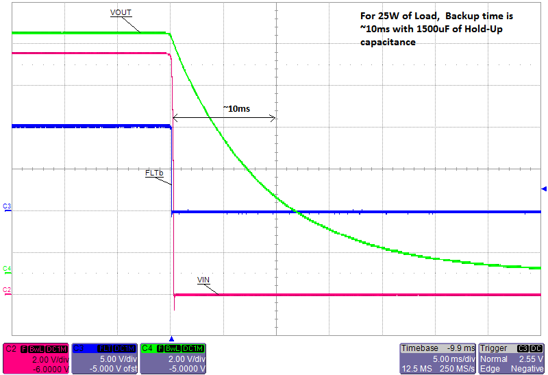
TPS25940 监视 V(IN) 和 V(OUT),以便在 V(IN) < (V(OUT) - 10mV) 时提供真正反向阻断。 这个功能在后备电压大于总线电压的系统中支持快速切换至一个升压储能元件。
- 如需了解所有可用封装,请见数据表末尾的可订购产品附录。
- TPS25940L = 已锁存,TPS25940A = 自动重试
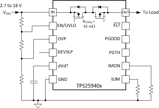
4 简化电路原理图
电源故障检测和阻断