ZHCSD51 December 2014 TPS2592BA , TPS2592BL
PRODUCTION DATA.
- 1 特性
- 2 应用
- 3 说明
- 4 应用电路原理图
- 5 修订历史记录
- 6 Device Comparison Table
- 7 Pin Configuration and Functions
- 8 Specifications
- 9 Detailed Description
-
10Application and Implementation
- 10.1 Application Information
- 10.2
Typical Applications
- 10.2.1
Simple 3.7-A eFuse Protection for Set Top Boxes
- 10.2.1.1 Design Requirements
- 10.2.1.2 Detailed Design Procedure
- 10.2.1.3 Support Component Selection - CVIN
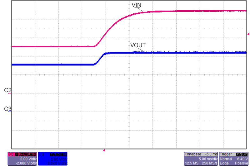
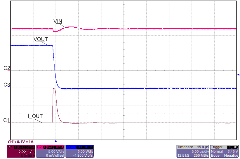
- 10.2.1.4 Application Curves
- 10.2.2 Inrush and Reverse Current Protection for Hold-Up Capacitor Application (e.g., SSD)
- 10.2.1
Simple 3.7-A eFuse Protection for Set Top Boxes
- 10.3 Maximum Device Power Dissipation Considerations
- 11Power Supply Recommendations
- 12Layout
- 13器件和文档支持
- 14机械封装和可订购信息
8 Specifications
8.1 Absolute Maximum Ratings
over operating temperature range (unless otherwise noted) (1)(2)| MIN | MAX | UNIT | ||
|---|---|---|---|---|
| Supply voltage range(1) | VIN | –0.3 | 20 | V |
| VIN (10 ms Transient) | 22 | |||
| Output voltage | OUT | –0.3 | VIN + 0.3 | V |
| OUT (Transient < 1 µs) | -1.2 | V | ||
| Voltage | ILIM | –0.3 | 7 | V |
| EN/UVLO | –0.3 | 7 | ||
| dV/dT | –0.3 | 7 | ||
| BFET | –0.3 | 30 | ||
| Continuous power dissipation | See the Thermal Information | |||
| Maximum power dissipation(3), PD = (VIN-VOUT)*ILIMIT |
TA = –40°C to +85°C | 40 | W | |
| TA = 0°C to +85°C | 50 | |||
| Storage temperature range, Tstg | -65 | 150 | °C | |
(1) Stresses beyond those listed under absolute maximum ratings may cause permanent damage to the device. These are stress ratings only and functional operation of the device at these or any conditions beyond those indicated under recommended operating conditions is not implied. Exposure to absolute-maximum-rated conditions for extended periods may affect device reliability.
(2) All voltage values, except differential voltages, are with respect to network ground terminal.
(3) Refer to detailed explanation in the application section Maximum Device Power Dissipation Considerations.
8.2 ESD Ratings
| VALUE | UNIT | |||
|---|---|---|---|---|
| V(ESD) | Electrostatic discharge | Human body model (HBM), per ANSI/ESDA/JEDEC JS-001(1) | ±2000 | V |
| Charged device model (CDM), per JEDEC specification JESD22-C101(2) | ±500 | |||
(1) JEDEC document JEP155 states that 500-V HBM allows safe manufacturing with a standard ESD control process.
(2) JEDEC document JEP157 states that 250-V CDM allows safe manufacturing with a standard ESD control process.
8.3 Recommended Operating Conditions
over operating free-air temperature range (unless otherwise noted)8.4 Thermal Information(1)
over operating free-air temperature range (unless otherwise noted)| THERMAL METRIC | TPS2592Bx | UNIT | |
|---|---|---|---|
| DRC (10) PINS | |||
| RθJA | Junction-to-ambient thermal resistance | 45.9 | °C/W |
| RθJCtop | Junction-to-case (top) thermal resistance | 53 | |
| RθJB | Junction-to-board thermal resistance | 21.2 | |
| ψJT | Junction-to-top characterization parameter | 1.2 | |
| ψJB | Junction-to-board characterization parameter | 21.4 | |
| RθJCbot | Junction-to-case (bottom) thermal resistance | 5.9 | |
(1) For more information about traditional and new thermal metrics, see the IC Package Thermal Metrics application report, SPRA953.
8.5 Electrical Characteristics
–40°C ≤ TJ ≤ 125°C, VIN = 5 V, VEN/UVLO = 2 V, RILIM = 100 kΩ, CdVdT = OPEN. All voltages referenced to GND (unless otherwise noted)| PARAMETER | TEST CONDITIONS | MIN | TYP | MAX | UNIT | |
|---|---|---|---|---|---|---|
| VIN (INPUT SUPPLY) | ||||||
| VUVR | UVLO threshold, rising | 4.15 | 4.3 | 4.45 | V | |
| VUVhyst | UVLO hysteresis(1) | 5.4% | ||||
| IQON | Supply current | Enabled: EN/UVLO = 2 V | 0.4 | 0.62 | 0.80 | mA |
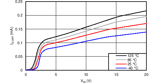
| IQOFF | EN/UVLO = 0 V | 0.1 | 0.25 | mA | ||
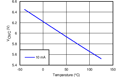
| VOVC | Over-voltage clamp | VIN > 6.75 V, IOUT = 10 mA, –40℃ ≤ TJ ≤ 85℃ |
5.5 | 6.1 | 6.75 | V |
| VIN > 6.75 V, IOUT = 10 mA, –40℃ ≤ TJ ≤ 125℃ |
5.25 | 6.1 | 6.75 | |||
| EN/UVLO (ENABLE/UVLO INPUT) | ||||||
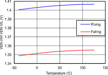
| VENR | EN Threshold voltage, rising | 1.37 | 1.4 | 1.44 | V | |
| VENF | EN Threshold voltage, falling | 1.32 | 1.35 | 1.39 | V | |
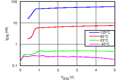
| IEN | EN Input leakage current | 0 V ≤ VEN ≤ 5 V | –100 | 0 | 100 | nA |
| dV/dT (OUTPUT RAMP CONTROL) | ||||||
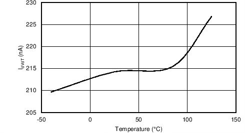
| IdVdT | dV/dT Charging current(1) | VdVdT = 0 V | 220 | nA | ||
| RdVdT_disch | dV/dT Discharging resistance | EN/UVLO = 0 V, IdVdT = 10 mA sinking | 50 | 73 | 100 | Ω |
| VdVdTmax | dV/dT Max capacitor voltage(1) | 5.5 | V | |||
| GAINdVdT | dV/dT to OUT gain(1) | ΔVdVdT | 4.85 | V/V | ||
| ILIM (CURRENT LIMIT PROGRAMMING) | ||||||
| IILIM | ILIM Bias current(1) | 10 | µA | |||
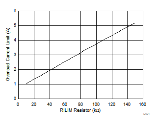
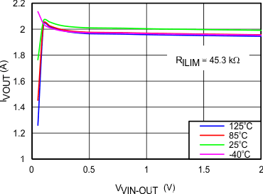
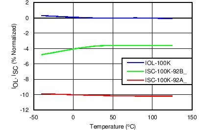
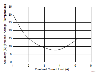
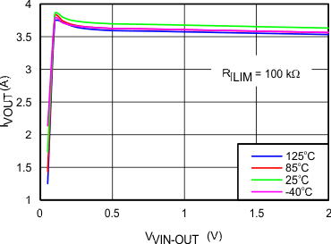
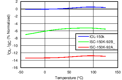
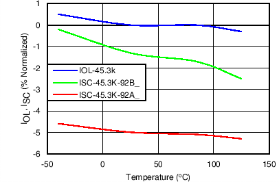
| IOL | Overload current limit(2) | RILIM = 45.3 kΩ, VVIN-OUT = 1 V | 1.79 | 2.10 | 2.42 | A |
| RILIM = 100 kΩ, VVIN-OUT = 1 V | 3.46 | 3.75 | 4.03 | |||
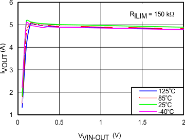
| RILIM = 150 kΩ, VVIN-OUT = 1 V | 4.4 | 5.2 | 6 | |||
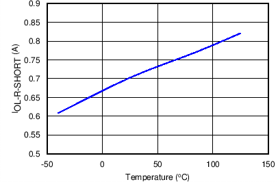
| IOL-R-Short | RILIM = 0 Ω, Shorted Resistor Current Limit (Single Point Failure Test: UL60950)(1) | 0.7 | A | |||
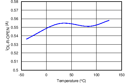
| IOL-R-Open | RILIM = OPEN, Open Resistor Current Limit (Single Point Failure Test: UL60950)(1) | 0.55 | A | |||
| ISCL | Short-circuit current limit(2) | RILIM = 45.3 kΩ, VVIN-OUT = 5 V | 1.72 | 2.05 | 2.38 | A |
| RILIM = 100 kΩ, VVIN-OUT = 5 V | 3.14 | 3.56 | 3.98 | |||
| RILIM = 150 kΩ, VVIN-OUT = 5 V | 4.12 | 4.86 | 5.60 | |||
| RATIOFASTRIP | Fast-Trip comparator level w.r.t. overload current limit(1) | IFASTRIP : IOL | 160% | |||
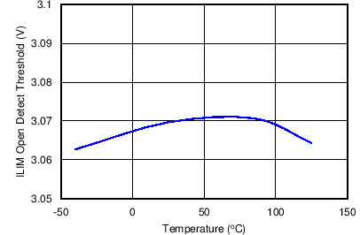
| VOpenILIM | ILIM Open resistor detect threshold(1) | VILIM Rising, RILIM = OPEN | 3.1 | V | ||
| OUT (PASS FET OUTPUT) | ||||||
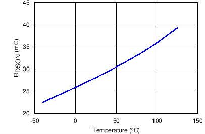
| RDS(on) | FET ON resistance | TJ = 25°C | 21 | 28 | 33 | mΩ |
| TJ = 125°C | 39 | 46 | ||||
| IOUT-OFF-LKG | OUT Bias current in off state | VEN/UVLO = 0 V, VOUT = 0 V (Sourcing) | –5 | 0 | 1 | µA |
| IOUT-OFF-SINK | VEN/UVLO = 0V, VOUT = 300 mV (Sinking) | 10 | 15 | 20 | ||
| BFET (BLOCKING FET GATE DRIVER) | ||||||
| IBFET | BFET Charging current(1) | VBFET = VOUT | 2 | µA | ||
| VBFETmax | BFET Clamp voltage(1) | VVIN + 6.4 | V | |||
| RBFETdisch | BFET Discharging resistance to GND | VEN/UVLO = 0 V, IBFET = 100 mA | 15 | 26 | 36 | Ω |
| TSD (THERMAL SHUT DOWN) | ||||||
| TSHDN | TSD Threshold, rising(1) | 160 | °C | |||
| TSHDNhyst | TSD Hysteresis(1) | 10 | °C | |||
| Thermal fault: latched or autoretry | TPS2592BL | LATCHED | ||||
| TPS2592BA | AUTO-RETRY | |||||
(1) These parameters are provided for reference only and do not constitute part of TI's published device specifications for purposes of TI's product warranty.
(2) Pulsed testing techniques used during this test maintain junction temperature approximately equal to ambient temperature.
8.6 Timing Requirements
| PARAMETER | TEST CONDITIONS | MIN | TYP | MAX | UNIT | |
|---|---|---|---|---|---|---|
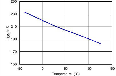
| TON | Turn-on delay(1) | EN/UVLO → H to IVIN = 100 mA, 1-A resistive load at OUT | 220 | µs | ||
| tOFFdly | Turn Off delay(1) | EN↓ to BFET↓, CBFET = 0 | 0.4 | µs | ||
| dV/dT (OUTPUT RAMP CONTROL) | ||||||
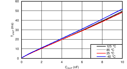
| tdVdT | Output ramp time | EN/UVLO → H to OUT = 4.9 V, CdVdT = 0 | 0.28 | 0.4 | 0.52 | ms |
| EN/UVLO → H to OUT = 4.9 V, CdVdT = 1 nF(1) |
5 | |||||
| ILIM (CURRENT LIMIT PROGRAMMING) | ||||||
| tFastOffDly | Fast-Trip comparator delay(1) | IOUT > IFASTRIP to IOUT= 0 (Switch Off) | 3 | µs | ||
| BFET (BLOCKING FET GATE DRIVER) | ||||||
| tBFET-ON | BFET Turn-On duration(1) | EN/UVLO → H to VBFET = 12 V, CBFET = 1 nF | 4.2 | ms | ||
| EN/UVLO → H to VBFET = 12 V, CBFET = 10 nF | 42 | |||||
| tBFET-OFF | BFET Turn-Off duration(1) | EN/UVLO → L to VBFET = 1 V, CBFET = 1 nF | 0.4 | µs | ||
| EN/UVLO → L to VBFET = 1 V, CBFET = 10 nF | 1.4 | |||||
(1) These parameters are provided for reference only and do not constitute part of TI's published device specifications for purposes of TI's product warranty.
8.7 Typical Characteristics
TJ = 25°C, VVIN = 5 V, VEN/UVLO = 2 V, RILIM = 100 kΩ, CVIN = 0.1 µF, COUT = 1 µF, CdVdT = OPEN (unless stated otherwise)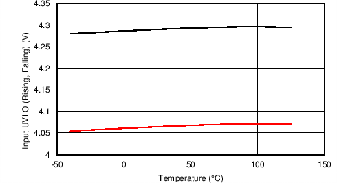

| TPS2592Bx | ||
| TPS2592Bx | ||

| TPS2592Bx, CdVdT = OPEN, COUT= 4.7 µF | ||

| EN ↓ | ||

| VIN↓ | ||
| 150 kΩ | ||
| 45.3 kΩ | ||
| 100 kΩ | ||
| RILIM = 0 | ||


| TPS2592BA | ||
| TPS2592Bx | ||
| TPS2592Bx | ||

| TPS2592Bx, CdVdT = 1 nF, COUT=10 µF, ROUT= 2.5 Ω | ||
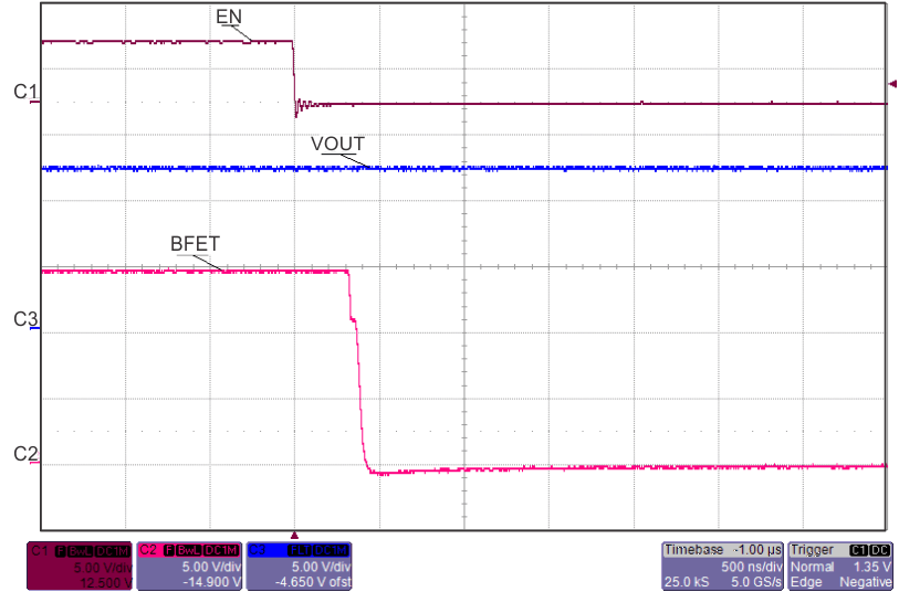
| EN↓ | ||
| 100 kΩ | ||
| 150 kΩ | ||
| 45.3 kΩ | ||
| RILIM = OPEN | ||


| ILOAD Stepped From 50% to 120%, back to 50% | ||

| TPS2592BL | ||