ZHCSTM4A October   2023  – March 2024 TPS25751

PRODUCTION DATA  

  1.   1
  2. 特性
  3. 应用
  4. 说明
  5. Device Comparison Table
  6. Pin Configuration and Functions
  7. Specifications
    1. 6.1  Absolute Maximum Ratings
      1. 6.1.1 TPS25751D and TPS25751S - Absolute Maximum Ratings
      2. 6.1.2 TPS25751D - Absolute Maximum Ratings
      3. 6.1.3 TPS25751S - Absolute Maximum Ratings
    2. 6.2  ESD Ratings
    3. 6.3  Recommended Operating Conditions
      1. 6.3.1 TPS25751D - Recommended Operating Conditions
      2. 6.3.2 TPS25751S - Recommended Operating Conditions
    4. 6.4  Recommended Capacitance
    5. 6.5  Thermal Information
      1. 6.5.1 TPS25751D - Thermal Information
      2. 6.5.2 TPS25751S - Thermal Information
    6. 6.6  Power Supply Characteristics
    7. 6.7  Power Consumption
    8. 6.8  PP_5V Power Switch Characteristics
    9. 6.9  PPHV Power Switch Characteristics - TPS25751D
    10. 6.10 PP_EXT Power Switch Characteristics - TPS25751S
    11. 6.11 Power Path Supervisory
    12. 6.12 CC Cable Detection Parameters
    13. 6.13 CC VCONN Parameters
    14. 6.14 CC PHY Parameters
    15. 6.15 Thermal Shutdown Characteristics
    16. 6.16 ADC Characteristics
    17. 6.17 Input/Output (I/O) Characteristics
    18. 6.18 BC1.2 Characteristics
    19. 6.19 I2C Requirements and Characteristics
    20. 6.20 Typical Characteristics
  8. Parameter Measurement Information
  9. Detailed Description
    1. 8.1 Overview
    2. 8.2 Functional Block Diagram
    3. 8.3 Feature Description
      1. 8.3.1  USB-PD Physical Layer
        1. 8.3.1.1 USB-PD Encoding and Signaling
        2. 8.3.1.2 USB-PD Bi-Phase Marked Coding
        3. 8.3.1.3 USB-PD Transmit (TX) and Receive (Rx) Masks
        4. 8.3.1.4 USB-PD BMC Transmitter
        5. 8.3.1.5 USB-PD BMC Receiver
        6. 8.3.1.6 Squelch Receiver
      2. 8.3.2  Power Management
        1. 8.3.2.1 Power-On And Supervisory Functions
        2. 8.3.2.2 VBUS LDO
      3. 8.3.3  Power Paths
        1. 8.3.3.1 Internal Sourcing Power Paths
          1. 8.3.3.1.1 PP_5V Current Clamping
          2. 8.3.3.1.2 PP_5V Local Overtemperature Shut Down (OTSD)
          3. 8.3.3.1.3 PP_5V OVP
          4. 8.3.3.1.4 PP_5V UVLO
          5. 8.3.3.1.5 PP_5Vx Reverse Current Protection
          6. 8.3.3.1.6 PP_CABLE Current Clamp
          7. 8.3.3.1.7 PP_CABLE Local Overtemperature Shut Down (OTSD)
          8. 8.3.3.1.8 PP_CABLE UVLO
        2. 8.3.3.2 TPS25751D Internal Sink Path
          1. 8.3.3.2.1 Overvoltage Protection (OVP)
          2. 8.3.3.2.2 Reverse-Current Protection (RCP)
          3. 8.3.3.2.3 VBUS UVLO
          4. 8.3.3.2.4 Discharging VBUS to Safe Voltage
        3. 8.3.3.3 TPS25751S - External Sink Path Control PP_EXT
          1. 8.3.3.3.1 Overvoltage Protection (OVP)
            1. 8.3.3.3.1.1 Reverse-Current Protection (RCP)
            2. 8.3.3.3.1.2 VBUS UVLO
            3. 8.3.3.3.1.3 Discharging VBUS to Safe Voltage
      4. 8.3.4  Cable Plug and Orientation Detection
        1. 8.3.4.1 Configured as a Source
        2. 8.3.4.2 Configured as a Sink
        3. 8.3.4.3 Configured as a DRP
        4. 8.3.4.4 Dead Battery Advertisement
      5. 8.3.5  Overvoltage Protection (CC1, CC2)
      6. 8.3.6  Default Behavior Configuration (ADCIN1, ADCIN2)
      7. 8.3.7  ADC
      8. 8.3.8  BC 1.2 (USB_P, USB_N)
      9. 8.3.9  Digital Interfaces
        1. 8.3.9.1 General GPIO
        2. 8.3.9.2 I2C Interface
      10. 8.3.10 Digital Core
      11. 8.3.11 I2C Interface
        1. 8.3.11.1 I2C Interface Description
          1. 8.3.11.1.1 I2C Clock Stretching
          2. 8.3.11.1.2 I2C Address Setting
          3. 8.3.11.1.3 Unique Address Interface
    4. 8.4 Device Functional Modes
      1. 8.4.1 Pin Strapping to Configure Default Behavior
      2. 8.4.2 Power States
    5. 8.5 Thermal Shutdown
  10. Application and Implementation
    1. 9.1 Application Information
    2. 9.2 Typical Application
      1. 9.2.1 Design Requirements
        1. 9.2.1.1 Programmable Power Supply (PPS) - Design Requirements
        2. 9.2.1.2 Liquid Detection Design Requirements
        3. 9.2.1.3 BC1.2 Application Design Requirements
        4. 9.2.1.4 USB Data Support Design Requirements
      2. 9.2.2 Detailed Design Procedure
        1. 9.2.2.1 Programmable Power Supply (PPS)
        2. 9.2.2.2 Liquid Detection
          1. 9.2.2.2.1 Liquid Detection Operation
        3. 9.2.2.3 BC1.2 Application
        4. 9.2.2.4 USB Data Support
      3. 9.2.3 Application Curves
        1. 9.2.3.1 Programmable Power Supply (PPS) Application Curves
        2. 9.2.3.2 Liquid Detection Application Curves
        3. 9.2.3.3 BC1.2 Application Curves
        4. 9.2.3.4 USB Data Support Application Curves
    3. 9.3 Power Supply Recommendations
      1. 9.3.1 3.3-V Power
        1. 9.3.1.1 VIN_3V3 Input Switch
      2. 9.3.2 1.5-V Power
      3. 9.3.3 Recommended Supply Load Capacitance
    4. 9.4 Layout
      1. 9.4.1 TPS25751D - Layout
        1. 9.4.1.1 Layout Guidelines
          1. 9.4.1.1.1 Recommended Via Size
          2. 9.4.1.1.2 Minimum Trace Widths
        2. 9.4.1.2 Layout Example
          1. 9.4.1.2.1 TPS25751D Schematic Layout Example
          2. 9.4.1.2.2 TPS25751D Layout Example - PCB Plots
            1. 9.4.1.2.2.1 TPS25751D Component Placement
            2. 9.4.1.2.2.2 TPS25751D PP5V
            3. 9.4.1.2.2.3 TPS25751D PPHV
            4. 9.4.1.2.2.4 TPS25751D VBUS
            5. 9.4.1.2.2.5 TPS25751D I/O (I2C, ADCINs, GPIOs)
            6. 9.4.1.2.2.6 TPS25751D DRAIN
            7. 9.4.1.2.2.7 TPS25751D GND
      2. 9.4.2 TPS25751S - Layout
        1. 9.4.2.1 Layout Guidelines
          1. 9.4.2.1.1 Recommended Via Size
          2. 9.4.2.1.2 Minimum Trace Widths
        2. 9.4.2.2 Layout Example
          1. 9.4.2.2.1 TPS25751S Schematic Layout Example
          2. 9.4.2.2.2 TPS25751S Layout Example - PCB Plots
            1. 9.4.2.2.2.1 TPS25751S Component Placement
            2. 9.4.2.2.2.2 TPS25751S PP5V
            3. 9.4.2.2.2.3 TPS25751S PP_EXT
            4. 9.4.2.2.2.4 TPS25751S VBUS
            5. 9.4.2.2.2.5 TPS25751S I/O
            6. 9.4.2.2.2.6 TPS25751S PPEXT Gate Driver
            7. 9.4.2.2.2.7 TPS25751S GND
  11. 10Device and Documentation Support
    1. 10.1 Device Support
      1. 10.1.1 第三方产品免责声明
      2. 10.1.2 Firmware Warranty Disclaimer
    2. 10.2 Documentation Support
      1. 10.2.1 Related Documentation
    3. 10.3 接收文档更新通知
    4. 10.4 支持资源
    5. 10.5 Trademarks
    6. 10.6 静电放电警告
    7. 10.7 术语表
  12. 11Revision History
  13. 12Mechanical, Packaging, and Orderable Information

封装选项

机械数据 (封装 | 引脚)
散热焊盘机械数据 (封装 | 引脚)
订购信息

USB Data Support Application Curves

The following show the control signals used by a USB SuperSpeed Mux. For a normal orientation, the CC1 pin is connected. For a flipped orientation, the CC2 pin is connected.

GUID-20230921-SS0I-PLPJ-FXQC-16MPMVRKMJFT-low.png Figure 9-23 USB SuperSpeed Mux Control - Normal Orientation
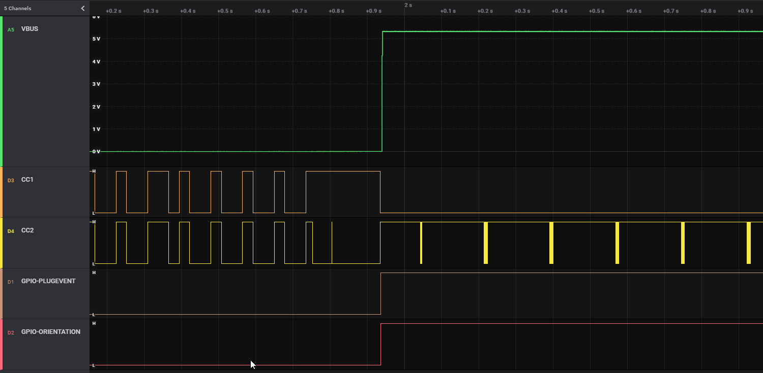
GUID-20230921-SS0I-51FD-01TM-DZ1ZQQCD6QQP-low.png Figure 9-24 USB SuperSpeed Mux Control - Flipped Orientation