ZHCSGV1C June   2017  – March 2018 TPS25740B

PRODUCTION DATA.  

  1. 特性
  2. 应用
  3. 说明
    1.     Device Images
      1.      简化原理图
  4. 修订历史记录
  5. Device Comparison Table
  6. Pin Configuration and Functions
    1.     Pin Functions
  7. Specifications
    1. 7.1 Absolute Maximum Ratings
    2. 7.2 ESD Ratings
    3. 7.3 Recommended Operating Conditions
    4. 7.4 Thermal Information
    5. 7.5 Electrical Characteristics
    6. 7.6 Timing Requirements
    7. 7.7 Switching Characteristics
    8. 7.8 Typical Characteristics
  8. Detailed Description
    1. 8.1 Overview
      1. 8.1.1 VBUS Capacitance
      2. 8.1.2 USB Data Communications
    2. 8.2 Functional Block Diagram
    3. 8.3 Feature Description
      1. 8.3.1  ENSRC
      2. 8.3.2  USB Type-C CC Logic (CC1, CC2)
      3. 8.3.3  USB PD BMC Transmission (CC1, CC2, VTX)
      4. 8.3.4  USB PD BMC Reception (CC1, CC2)
      5. 8.3.5  Discharging (DSCG, VPWR)
        1. 8.3.5.1 Discharging after a Fault (VPWR)
      6. 8.3.6  Configuring Voltage Capabilities (HIPWR)
      7. 8.3.7  Configuring Power Capabilities (PSEL, PCTRL, HIPWR)
      8. 8.3.8  Gate Driver (GDNG, GDNS)
      9. 8.3.9  Fault Monitoring and Protection
        1. 8.3.9.1 Over/Under Voltage (VBUS)
        2. 8.3.9.2 Over-Current Protection (ISNS, VBUS)
        3. 8.3.9.3 System Fault Input (GD, VPWR)
      10. 8.3.10 Voltage Control (CTL1, CTL2,CTL3)
      11. 8.3.11 Sink Attachment Indicator (DVDD)
      12. 8.3.12 Power Supplies (VAUX, VDD, VPWR, DVDD)
      13. 8.3.13 Grounds (AGND, GND)
      14. 8.3.14 Output Power Supply (DVDD)
    4. 8.4 Device Functional Modes
      1. 8.4.1 Sleep Mode
      2. 8.4.2 Checking VBUS at Start Up
  9. Application and Implementation
    1. 9.1 Application Information
      1. 9.1.1 System-Level ESD Protection
      2. 9.1.2 Using ENSRC to Enable the Power Supply upon Sink Attachment
      3. 9.1.3 Use of GD Internal Clamp
      4. 9.1.4 Resistor Divider on GD for Programmable Start Up
      5. 9.1.5 Selection of the CTL1, CTL2, and CTL3 Resistors (R(FBL1), R(FBL2), and R(FBL3))
      6. 9.1.6 Voltage Transition Requirements
      7. 9.1.7 VBUS Slew Control using GDNG C(SLEW)
      8. 9.1.8 Tuning OCP using RF and CF
    2. 9.2 Typical Applications
      1. 9.2.1 Typical Application, A/C Power Source (Wall Adapter)
        1. 9.2.1.1 Design Requirements
        2. 9.2.1.2 Detailed Design Procedure
          1. 9.2.1.2.1 Power Pin Bypass Capacitors
          2. 9.2.1.2.2 Non-Configurable Components
          3. 9.2.1.2.3 Configurable Components
        3. 9.2.1.3 Application Curves
      2. 9.2.2 Typical Application, D/C Power Source
        1. 9.2.2.1 Design Requirements
        2. 9.2.2.2 Detailed Design Procedure
          1. 9.2.2.2.1 Power Pin Bypass Capacitors
          2. 9.2.2.2.2 Non-Configurable Components
          3. 9.2.2.2.3 Configurable Components
        3. 9.2.2.3 Application Curves
    3. 9.3 System Examples
      1. 9.3.1 D/C Power Source (Power Hub)
      2. 9.3.2 A/C Power Source (Wall Adapter)
      3. 9.3.3 Dual-Port A/C Power Source (Wall Adaptor)
      4. 9.3.4 D/C Power Source (Power Hub with 3.3 V Rail)
  10. 10Power Supply Recommendations
    1. 10.1 VDD
    2. 10.2 VPWR
  11. 11Layout
    1. 11.1 Port Current Kelvin Sensing
    2. 11.2 Layout Guidelines
      1. 11.2.1 Power Pin Bypass Capacitors
      2. 11.2.2 Supporting Components
    3. 11.3 Layout Example
  12. 12器件和文档支持
    1. 12.1 文档支持
    2. 12.2 接收文档更新通知
    3. 12.3 社区资源
    4. 12.4 商标
    5. 12.5 静电放电警告
    6. 12.6 术语表
  13. 13机械、封装和可订购信息

封装选项

机械数据 (封装 | 引脚)
散热焊盘机械数据 (封装 | 引脚)
订购信息

Typical Characteristics

TPS25740B D004_SLVSDG8.gif
I(DSCG) = 100 mA
Figure 9. V(DSCG) while V(VPWR) > 4.65 V after an unplug
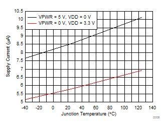
TPS25740B D006_SLVSDG8.gif
Figure 11. Supply Current While CC pins Unattached
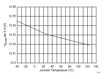
TPS25740B D008_SLVSDG8.gif
Figure 13. V(FOVP) While Supplying 9 V
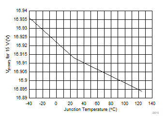
TPS25740B D010_SLVSDG8.gif
Figure 15. V(FOVP) While Supplying 15 V
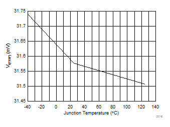
TPS25740B D016_SLVSDG8.gif
5 A enabled
Figure 17. VI(TRIP) When V(VPWR) > 4.65 V
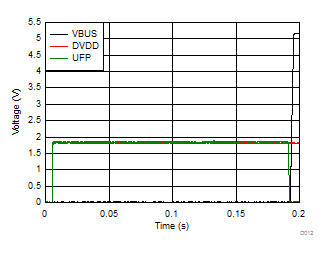
TPS25740B D012_SLVSDG8.gif
Sink attached at time 0
Figure 19. DVDD and ENSRC Upon Sink Attachment
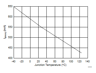
TPS25740B D005_SLVSDG8.gif
V(DSCG) = 4 V Pulsed Testing
Figure 10. I(DSCG) while V(VPWR) > 4.65 V after an unplug
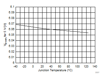
TPS25740B D007_SLVSDG8.gif
Figure 12. V(FOVP) While Supplying 5 V
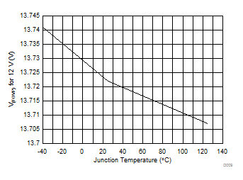
TPS25740B D009_SLVSDG8.gif
Figure 14. V(FOVP) While Supplying 12 V
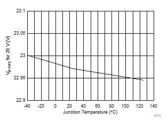
TPS25740B D015_SLVSDG8.gif
Figure 16. V(FOVP) While Supplying 20 V
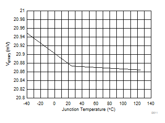
TPS25740B D011_SLVSDG8.gif
3 A enabled
Figure 18. VI(TRIP) When V(VPWR) > 4.65 V
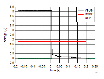
TPS25740B D013_SLVSDG8.gif
Sink detached at time 0s
Sleep mode entered at time 0.19s.
Figure 20. DVDD and ENSRC Upon Sink Attachment