ZHCSC59A March 2014 – June 2014 TPS2561A-Q1
PRODUCTION DATA.
- 1 特性
- 2 应用范围
- 3 说明
- 4 修订历史记录
- 5 Device Comparison Table
- 6 Pin Functions and Configurations
- 7 Specifications
- 8 Parameter Measurement Information
- 9 Detailed Description
-
10Application and Implementation
- 10.1 Application Information
- 10.2
Typical Application
- 10.2.1
Design Current Limit
- 10.2.1.1 Design Requirements
- 10.2.1.2
Detailed Design Procedure
- 10.2.1.2.1 Determine Design Parameters
- 10.2.1.2.2 Programming the Current-Limit Threshold
- 10.2.1.2.3 Designing Above a Minimum Current Limit
- 10.2.1.2.4 Designing Below a Maximum Current Limit
- 10.2.1.2.5 Accounting for Resistor Tolerance
- 10.2.1.2.6 Power Dissipation and Junction Temperature
- 10.2.1.2.7 Auto-Retry Functionality
- 10.2.1.2.8 Two-Level Current-Limit Circuit
- 10.2.2 Application Curves
- 10.2.1
Design Current Limit
- 11Power Supply Requirements
- 12Layout
- 13器件和文档支持
- 14机械封装和可订购信息
7 Specifications
7.1 Absolute Maximum Ratings
over operating free-air temperature range unless otherwise noted(1)(2)| MIN | MAX | UNIT | |||
|---|---|---|---|---|---|
| Voltage range on IN, OUTx, ENx, ILIM, FAULTx | –0.3 | 7 | V | ||
| Voltage range from IN to OUTx | –7 | 7 | V | ||
| Continuous output current | Internally Limited | ||||
| Continuous FAULTx sink current | 25 | mA | |||
| ILIM source current | Internally Limited | mA | |||
| TJ | Maximum junction temperature | –40 | Internally Limited | °C | |
(1) Stresses beyond those listed under absolute maximum ratings may cause permanent damage to the device. These are stress ratings only, and functional operation of the device at these or any other conditions beyond those indicated under recommended operating conditions is not implied. Exposure to absolute-maximum-rated conditions for extended periods may affect device reliability.
(2) Voltages are referenced to GND unless otherwise noted.
7.2 Handling Ratings
| MIN | MAX | UNIT | |||
|---|---|---|---|---|---|
| TSTG | Storage temperature range | -65 | 150 | °C | |
| VESD(1) | Human Body Model (HBM) | AEC-Q100 Classification Level H2 | 2 | kV | |
| Charged Device Model (CDM) | AEC-Q100 Classification Level C5 | 750 | V | ||
| System level (contact/air) | 8/15(2) | kV | |||
(1) Electrostatic discharge (ESD) to measure device sensitivity and immunity to damage caused by assembly line electrostatic discharges in to the device.
(2) Surges per EN61000-4-2, 1999 applied between USB connection for VBUS and GND of the TPS2560EVM (HPA424, replacing TPS2560 with TPS2561A-Q1) evaluation module (documentation available on the Web.) These were the test level, no the failure threshold.
7.3 Recommended Operating Conditions
| MIN | MAX | UNIT | |||
|---|---|---|---|---|---|
| VIN | Input voltage, IN | 2.5 | 6.5 | V | |
| VENx | Enable voltage | 0 | 6.5 | V | |
| VIH | High-level input voltage on ENx | 1.1 | V | ||
| VIL | Low-level input voltage on ENx | 0.66 | |||
| IOUTx | Continuous output current per channel, OUTx | 0 | 2.5 | A | |
| Continuous FAULTx sink current | 0 | 10 | mA | ||
| TJ | Operating junction temperature | –40 | 125 | °C | |
| RILIM | Recommended resistor limit range | 20 | 187 | kΩ | |
7.4 Thermal Information(1)
| THERMAL METRIC | TPS2561A-Q1 | UNIT | |
|---|---|---|---|
| DRC (10 TERMINALS) | |||
| θJA | Junction-to-ambient thermal resistance | 38.1 | °C/W |
| θJCtop | Junction-to-case (top) thermal resistance | 40.5 | |
| θJB | Junction-to-board thermal resistance | 13.6 | |
| ψJT | Junction-to-top characterization parameter | 0.6 | |
| ψJB | Junction-to-board characterization parameter | 13.7 | |
| θJCbot | Junction-to-case (bottom) thermal resistance | 3.4 | |
(1) For more information about traditional and new thermal metrics, see the IC Package Thermal Metrics application report, SPRA953.
7.5 Electrical Characteristics
over recommended operating conditions, VENx = VIN (unless otherwise noted)| PARAMETER | TEST CONDITIONS(1) | MIN | TYP | MAX | UNIT | ||||
|---|---|---|---|---|---|---|---|---|---|
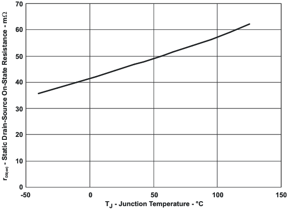
| POWER SWITCH | |||||||||
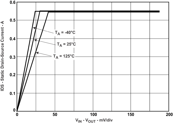
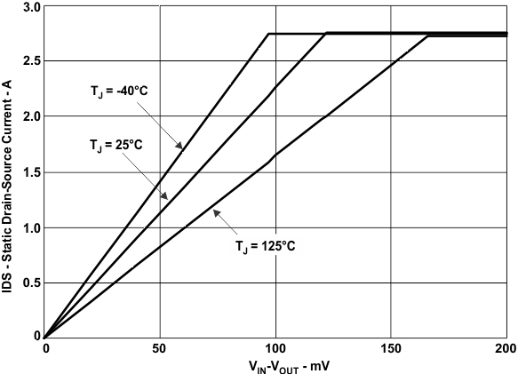
| rDS(on) | Static drain-source on-state resistance per channel, IN to OUTx | TJ = 25°C | 44 | 50 | mΩ | ||||
| –40°C ≤TJ ≤125 °C | 70 | ||||||||
| tr | Rise time, output | VIN = 6.5 V | CLx = 1 μF, RLx = 100 Ω, (see Figure 9) |
1.5 | 3 | 4 | ms | ||
| VIN = 2.5 V | 0.5 | 2 | 3 | ||||||
| tf | Fall time, output | VIN = 6.5 V | 0.5 | 0.8 | 1.0 | ||||
| VIN = 2.5 V | 0.3 | 0.6 | 0.8 | ||||||
| ENABLE INPUT EN | |||||||||
| Enable pin turn on/off threshold | 0.66 | 1.1 | V | ||||||
| Hysteresis | 55(2) | mV | |||||||
| IEN | Input current | VENx = 0 V or 6.5 V | –0.5 | 0.5 | μA | ||||
| ton | Turnon time | CLx = 1 μF, RLx = 100 Ω, (see Figure 9) | 9 | ms | |||||
| toff | Turnoff time | 6 | ms | ||||||
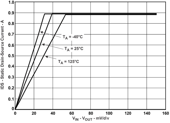
| CURRENT LIMIT | |||||||||
| IOS | Current-limit (see Figure 11) | OUTx connected to GND | RILIM = 20 kΩ | 2560 | 2750 | 2980 | mA | ||
| RILIM = 24.3 kΩ | 2100 | 2250 | 2500 | ||||||
| RILIM = 61.9 kΩ | 800 | 900 | 1005 | ||||||
| RILIM = 100 kΩ | 470 | 560 | 645 | ||||||
| OUT1 and OUT2 connected to GND | RILIM = 47.5 kΩ | 2100 | 2300 | 2500 | |||||
| tIOS | Response time to short circuit | VIN = 5 V (see Figure 10) | 3.5(2) | μs | |||||
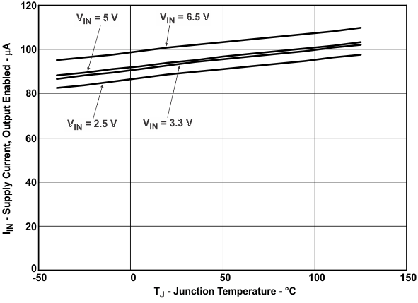
| SUPPLY CURRENT | |||||||||
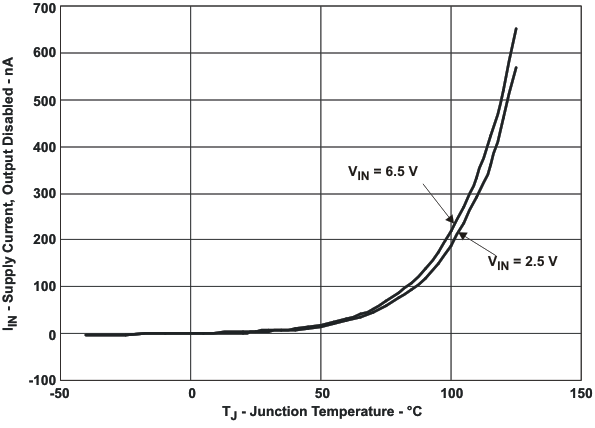
| IIN(off) | Supply current, low-level output | VIN = 6.5 V, No load on OUTx, VENx = 0 V | 0.1 | 2.0 | μA | ||||
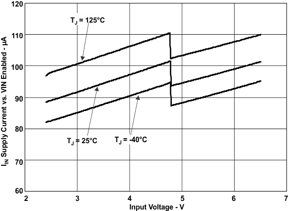
| IIN(on) | Supply current, high-level output | VIN = 6.5 V, No load on OUT | RILIM = 20 kΩ | 100 | 125 | μA | |||
| RILIM = 100 kΩ | 85 | 110 | μA | ||||||
| IREV | Reverse leakage current | VOUTx = 6.5 V, VIN = 0 V | TJ = 25°C | 0.01 | 1.0 | μA | |||
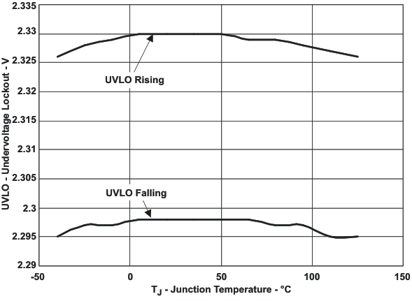
| UNDERVOLTAGE LOCKOUT | |||||||||
| VUVLO | Low-level input voltage, IN | VIN rising | 2.35 | 2.45 | V | ||||
| Hysteresis, IN | TJ = 25°C | 35(2) | mV | ||||||
| FAULTx FLAG | |||||||||
| VOL | Output low voltage, FAULTx | IFAULTx = 1 mA | 180 | mV | |||||
| Off-state leakage | VFAULTx = 6.5 V | 1 | μA | ||||||
| FAULTx deglitch | FAULTx assertion or de-assertion due to overcurrent condition | 6 | 9 | 13 | ms | ||||
| THERMAL SHUTDOWN | |||||||||
| Thermal shutdown threshold, OTSD2 | 155 | °C | |||||||
| Thermal shutdown threshold in current-limit, OTSD | 135 | °C | |||||||
| Hysteresis | 20(2) | °C | |||||||
(1) Pulse-testing techniques maintain junction temperature close to ambient temperature; thermal effects must be taken into account separately.
(2) These parameters are provided for reference only, and do not constitute part of TI's published specifications for purposes of TI's product warranty.
7.6 Typical Characteristics
| RLIM = 20 kΩ |
| RLIM = 61.9 kΩ |
| RLIM = 20 kΩ |
| RLIM = 100 kΩ |
| RLIM = 20 kΩ |