ZHCSC59A March 2014 – June 2014 TPS2561A-Q1
PRODUCTION DATA.
- 1 特性
- 2 应用范围
- 3 说明
- 4 修订历史记录
- 5 Device Comparison Table
- 6 Pin Functions and Configurations
- 7 Specifications
- 8 Parameter Measurement Information
- 9 Detailed Description
-
10Application and Implementation
- 10.1 Application Information
- 10.2
Typical Application
- 10.2.1
Design Current Limit
- 10.2.1.1 Design Requirements
- 10.2.1.2
Detailed Design Procedure
- 10.2.1.2.1 Determine Design Parameters
- 10.2.1.2.2 Programming the Current-Limit Threshold
- 10.2.1.2.3 Designing Above a Minimum Current Limit
- 10.2.1.2.4 Designing Below a Maximum Current Limit
- 10.2.1.2.5 Accounting for Resistor Tolerance
- 10.2.1.2.6 Power Dissipation and Junction Temperature
- 10.2.1.2.7 Auto-Retry Functionality
- 10.2.1.2.8 Two-Level Current-Limit Circuit
- 10.2.2 Application Curves
- 10.2.1
Design Current Limit
- 11Power Supply Requirements
- 12Layout
- 13器件和文档支持
- 14机械封装和可订购信息
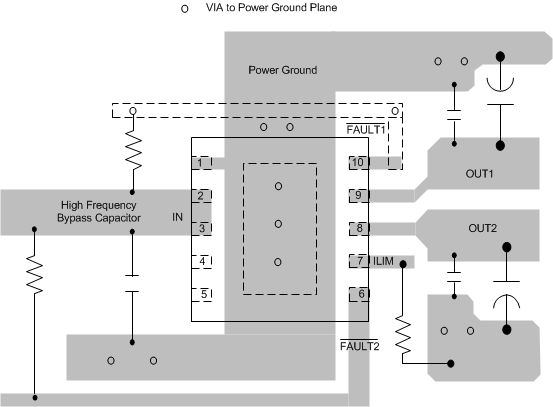
12 Layout
12.1 Layout Guidelines
For all applications, a 0.1-µF or greater ceramic bypass capacitor between IN and GND is recommended as close to the device as possible for local noise decoupling. This precaution reduces ringing on the input due to power-supply transients. Additional input capacitance may be needed on the input to reduce voltage overshoot form exceeding the absolute-maximum voltage of the device during heavy transient conditions.
- Output capacitance is not required, but placing a high-value electrolytic capacitor on the output pin is recommended when large transient currents are expected on the output.
- The traces routing the RILIM resistor to the device should be as short as possible to reduce parasitic effects on the current limit accuracy.
- The PowerPAD™ should be directly connected to PCB ground plane using wide and short copper trace.
12.2 Layout Example