ZHCSCR7A June   2014  – November 2020 TPS2559

PRODUCTION DATA  

  1. 特性
  2. 应用
  3. 说明
  4. Revision History
  5. Device Comparison Table
  6. Pin Configuration and Functions
  7. Specifications
    1. 7.1 Absolute Maximum Ratings
    2. 7.2 ESD Ratings
    3. 7.3 Recommended Operating Conditions
    4. 7.4 Thermal Information
    5. 7.5 Electrical Characteristics
    6. 7.6 Timing Requirements
    7. 7.7 Timing Diagrams
    8. 7.8 Typical Characteristics
  8. Detailed Description
    1. 8.1 Overview
    2. 8.2 Functional Block Diagram
    3. 8.3 Feature Description
      1. 8.3.1 Thermal Sense
      2. 8.3.2 Overcurrent Protection
      3. 8.3.3 FAULT Response
    4. 8.4 Device Functional Modes
      1. 8.4.1 Operation with VIN Undervoltage Lockout (UVLO) Control
      2. 8.4.2 Operation with EN Control
  9. Application and Implementation
    1. 9.1 Application Information
    2. 9.2 Typical Application
      1. 9.2.1 Design Requirements
      2. 9.2.2 Detailed Design Procedure
        1. 9.2.2.1 Step-by-Step Design Procedure
        2. 9.2.2.2 Input and Output Capacitance
        3. 9.2.2.3 Programming the Current-Limit Threshold
        4. 9.2.2.4 Design Above a Minimum Current Limit
        5. 9.2.2.5 Design Below a Maximum Current Limit
        6. 9.2.2.6 Accounting for Resistor Tolerance
        7. 9.2.2.7 Power Dissipation and Junction Temperature
        8. 9.2.2.8 Auto-Retry
        9. 9.2.2.9 Two-Level Current-Limit
      3. 9.2.3 Application Curves
  10. 10Power Supply Recommendations
  11. 11Layout
    1. 11.1 Layout Guidelines
    2. 11.2 Layout Example
  12. 12Device and Documentation Support
    1. 12.1 Receiving Notification of Documentation Updates
    2. 12.2 Support Resources
    3. 12.3 Trademarks
    4. 12.4 Electrostatic Discharge Caution
    5. 12.5 Glossary
  13. 13Mechanical, Packaging, and Orderable Information

封装选项

机械数据 (封装 | 引脚)
散热焊盘机械数据 (封装 | 引脚)
订购信息

Application Curves

GUID-235167ED-855B-40F6-BEE7-0E70020CF0F4-low.png
 
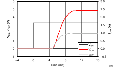
Figure 9-6 Output Rise With 150 µF // 5 Ω
GUID-DC657E8C-164D-4465-826A-FA34FF56AFCB-low.png
 
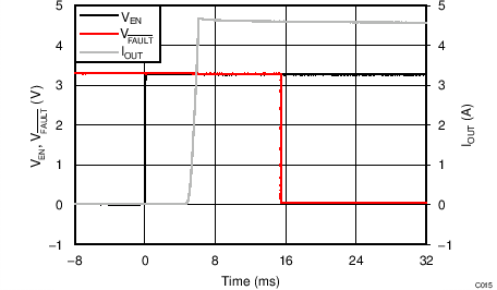
Figure 9-8 Enable Into Output Short
GUID-66A44952-8188-406E-892F-CAF718408A4E-low.png
 
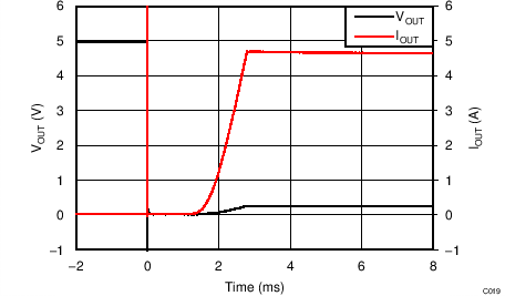
Figure 9-10 Output Short to Full Load Recovery Response
GUID-FE215657-4D18-4E95-A642-33DE2084F7AF-low.png
 
Figure 9-12 50-mΩ Hot-Short Response Time
GUID-EA4F9AD0-26F4-4F29-B86D-31ACFB2EE079-low.png
 
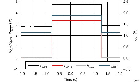
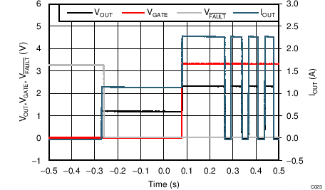
Figure 9-14 Two-Level Current Limit With RLOAD = 2.5 Ω
GUID-18731370-CB97-4628-9358-A49CEC5D9E15-low.png
 
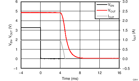
Figure 9-7 Output Fall With 150 µF // 5 Ω
GUID-71C013B2-99E3-4299-AD87-B33B4F0D93BC-low.png
 
Figure 9-9 Full Load to Output Short Transient Response
GUID-9F14B67E-3922-41C9-BFB4-41B488E5065E-low.png
 
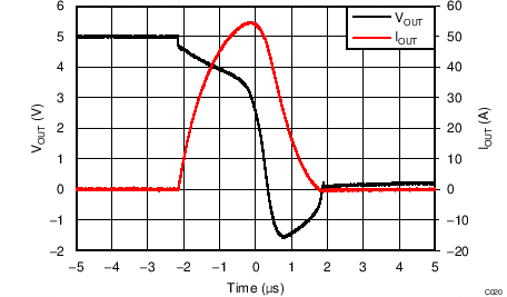
Figure 9-11 50-mΩ Hot-Short
GUID-2F8ECD7C-D0BD-40CB-9562-5A934CAD0859-low.png
 
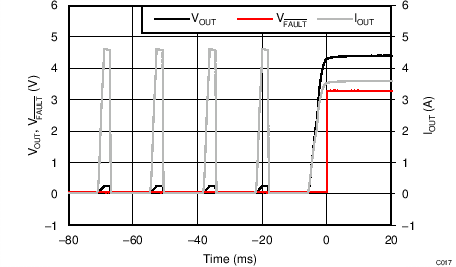
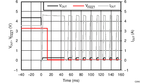
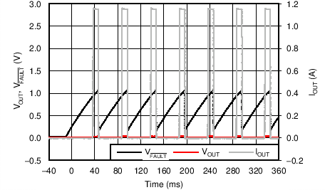
Figure 9-13 Auto-Retry Cycle
GUID-667E648A-748C-4CA3-A098-B42893766D12-low.png
 
Figure 9-15 Two-Level Current Limit With RLOAD = 1 Ω