ZHCSMB5A March   2021  – March 2022 TPS2521

PRODUCTION DATA  

  1. 特性
  2. 应用
  3. 说明
  4. Revision History
  5. Device Comparison Table
  6. Pin Configuration and Functions
  7. Specifications
    1. 7.1 Absolute Maximum Ratings
    2. 7.2 ESD Ratings
    3. 7.3 Recommended Operating Conditions
    4. 7.4 Thermal Information
    5. 7.5 Electrical Characteristics
    6. 7.6 Timing Requirements
    7. 7.7 Switching Characteristics
      1.      15
    8. 7.8 Typical Characteristics
  8. Detailed Description
    1. 8.1 Overview
    2. 8.2 Functional Block Diagram
    3. 8.3 Feature Description
      1. 8.3.1 Input Reverse Polarity Protection
      2. 8.3.2 Undervoltage Lockout (UVLO and UVP)
      3. 8.3.3 Overvoltage Clamp (OVC)
      4. 8.3.4 Inrush Current, Overcurrent, and Short Circuit Protection
        1. 8.3.4.1 Slew Rate (dVdt) and Inrush Current Control
        2. 8.3.4.2 Active Current Limiting
        3. 8.3.4.3 Short-Circuit Protection
      5. 8.3.5 Analog Load Current Monitor
      6. 8.3.6 Reverse Current Protection
      7. 8.3.7 Overtemperature Protection (OTP)
      8. 8.3.8 Fault Response
      9. 8.3.9 Power Good Indication (PG)
    4. 8.4 Device Functional Modes
  9. Application and Implementation
    1. 9.1 Application Information
    2. 9.2 Single Device, Self-Controlled
    3. 9.3 Typical Application
      1. 9.3.1 Application
      2. 9.3.2 Design Requirements
      3. 9.3.3 Detailed Design Procedure
        1. 9.3.3.1 Device Selection
        2. 9.3.3.2 Setting Undervoltage and Overvoltage Thresholds
        3. 9.3.3.3 Setting Output Voltage Rise Time (tR)
        4. 9.3.3.4 Setting Power Good Assertion Threshold
        5. 9.3.3.5 Setting Overcurrent Threshold (ILIM)
        6. 9.3.3.6 Setting Overcurrent Blanking Interval (tITIMER)
      4. 9.3.4 Application Curves
  10. 10Power Supply Recommendations
    1. 10.1 Transient Protection
    2. 10.2 Output Short-Circuit Measurements
  11. 11Layout
    1. 11.1 Layout Guidelines
    2. 11.2 Layout Example
  12. 12Device and Documentation Support
    1. 12.1 Documentation Support
      1. 12.1.1 Related Documentation
    2. 12.2 接收文档更新通知
    3. 12.3 支持资源
    4. 12.4 Trademarks
    5. 12.5 Electrostatic Discharge Caution
    6. 12.6 术语表
  13. 13Mechanical, Packaging, and Orderable Information

封装选项

机械数据 (封装 | 引脚)
散热焊盘机械数据 (封装 | 引脚)
订购信息

Setting Undervoltage and Overvoltage Thresholds

The supply undervoltage threshold is set using the resistors R1, R2 and can be calculated using Equation 7:

Equation 7. GUID-20210324-CA0I-74FX-DNP3-HG8SRRVXWRZ4-low.gif
VUVLO(R) is the UVLO rising threshold. Because R1 and R2 leak the current from input supply VIN, these resistors must be selected based on the acceptable leakage current from input power supply VIN. The current drawn by R1 and R2 from the power supply is IR12 = VIN / (R1 + R2 ). However, leakage currents due to external active components connected to the resistor string can add error to these calculations. So, the resistor string current, IR12 must be chosen to be 20 times greater than the leakage current expected on the EN/UVLO pin.

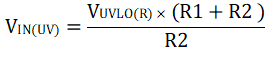
From the device electrical specifications, the EN/UVLO leakage current is 0.1 μA (maximum), and VUVLO(R) = 1.2 V. From design requirements,VIN(UV) = 4 V. To solve the equation, first choose the value of R1 = 470 kΩ and use the above equation to solve for R2 = 201.4 kΩ.

Using the closest standard 1% resistor values, we get R1 = 470 kΩ and R2 = 205 kΩ.

Refer to Table 8-5 to set overvoltage clamp. OVCSEL pin is left open to select overvoltage clamp as 5.7 V.