SPAS093C December 2009 – September 2015 TPS2505
PRODUCTION DATA.
- 1 Features
- 2 Applications
- 3 Description
- 4 Revision History
- 5 Pin Configuration and Functions
-
6 Specifications
- 6.1 Absolute Maximum Ratings
- 6.2 ESD Ratings
- 6.3 Recommended Operating Conditions
- 6.4 Thermal Information
- 6.5 Electrical Characteristics (Shared Boost, LDO and USB)
- 6.6 Electrical Characteristics (Boost Only)
- 6.7 Electrical Characteristics (USB1/2 Only)
- 6.8 Electrical Characteristics (LDO and Reset Only)
- 6.9 Recommended External Components
- 6.10 Dissipation Ratings
- 6.11 Typical Characteristics
- 7 Parameter Measurement Information
-
8 Detailed Description
- 8.1 Overview
- 8.2 Functional Block Diagram
- 8.3
Feature Description
- 8.3.1 PGND
- 8.3.2 IN
- 8.3.3 EN
- 8.3.4 GND
- 8.3.5 ILIM1/2
- 8.3.6 RESET
- 8.3.7 LDOOUT
- 8.3.8 LDOIN
- 8.3.9 ENLDO
- 8.3.10 FAULT1/2
- 8.3.11 ENUSB1/2
- 8.3.12 USB1/2
- 8.3.13 AUX
- 8.3.14 SW
- 8.3.15 Thermal Pad
- 8.3.16 Boost Converter
- 8.3.17 USB Switches
- 8.3.18 3.3-V LDO
- 8.3.19 Reset Comparator
- 8.3.20 Thermal Shutdown
- 8.3.21 Component Recommendations
- 8.4 Device Functional Modes
-
9 Application and Implementation
- 9.1 Application Information
- 9.2
Typical Application
- 9.2.1 Design Requirements
- 9.2.2 Detailed Design Procedure
- 9.2.3 Application Curves
- 10Power Supply Recommendations
- 11Layout
- 12Device and Documentation Support
- 13Mechanical, Packaging, and Orderable Information
6 Specifications
6.1 Absolute Maximum Ratings
Over operating free-air temperature range (unless otherwise noted).(1)(2)| MIN | MAX | UNIT | ||
|---|---|---|---|---|
| Input voltage on SW, AUX, IN, USB, ENUSB, EN, FAULT, ILIM | –0.3 | 7 | V | |
| FAULT sink current | 25 | mA | ||
| ILIM source current | 1 | mA | ||
| Operating junction temperature, TJ | –40 | 125 | °C | |
| Storage temperature, Tstg | –65 | 150 | °C | |
(1) Stresses beyond those listed under Absolute Maximum Ratings may cause permanent damage to the device. These are stress ratings only and functional operation of the device at these or any other conditions beyond those indicated under Recommended Operating Conditions is not implied. Exposure to absolute-maximum-rated conditions for extended periods may affect device reliability.
(2) Voltages are referenced to GND and PGND tied together.
6.2 ESD Ratings
| VALUE | UNIT | ||||
|---|---|---|---|---|---|
| V(ESD) | Electrostatic discharge | Human body model (HBM), per ANSI/ESDA/JEDEC JS-001, all pins(1) | ±2000 | V | |
| Charged device model (CDM), per JEDEC specification JESD22-C101, all pins(2) | ±500 | ||||
(1) JEDEC document JEP155 states that 500-V HBM allows safe manufacturing with a standard ESD control process.
(2) JEDEC document JEP157 states that 250-V CDM allows safe manufacturing with a standard ESD control process.
6.3 Recommended Operating Conditions
over operating free-air temperature range (unless otherwise noted)| MIN | MAX | UNIT | |||
|---|---|---|---|---|---|
| VIN | Supply voltage at IN | 1.8 | 5.25 | V | |
| VSTART | Supply voltage at IN for start-up | 2.2 | V | ||
| Enable voltage at EN, ENUSB1, ENUSB2, ENLDO | 0 | 5.25 | V | ||
| TA | Operating free air temperature range | –40 | 85 | °C | |
| TJ | Operating junction temperature range | –40 | 125 | °C | |
6.4 Thermal Information
| THERMAL METRIC(1) | TPS2505 | UNIT | |
|---|---|---|---|
| RGW (VQFN) | |||
| 20 PINS | |||
| RθJA | Junction-to-ambient thermal resistance | 34.3 | °C/W |
| RθJC(top) | Junction-to-case (top) thermal resistance | 30 | °C/W |
| RθJB | Junction-to-board thermal resistance | 13.5 | °C/W |
| ψJT | Junction-to-top characterization parameter | 0.4 | °C/W |
| ψJB | Junction-to-board characterization parameter | 13.5 | °C/W |
| RθJC(bot) | Junction-to-case (bottom) thermal resistance | 3.1 | °C/W |
(1) For more information about traditional and new thermal metrics, see the Semiconductor and IC Package Thermal Metrics application report, SPRA953.
6.5 Electrical Characteristics (Shared Boost, LDO and USB)
over recommended operating conditions (unless otherwise noted)| PARAMETER | TEST CONDITIONS | MIN | TYP | MAX | UNIT | |||
|---|---|---|---|---|---|---|---|---|
| BIAS | ||||||||
| Bias Current | VIN | VIN = 3.3 V, VAUX = 5.2 V, VEN = VIN, VENUSB1 = VAUX, IAUX = IUSB = 0 A |
15 | 25 | µA | |||
| VAUX | 500 | 600 | ||||||
| Shutdown current | VIN | VIN = 3.3 V, VEN = VENUSB = 0 V, AUX and USB OPEN, –40°C ≤ TJ ≤ 85°C |
5 | µA | ||||
| UVLO | ||||||||
| Undervoltage lockout threshold on IN for boost converter | VIN rising | 2.08 | 2.20 | V | ||||
| VIN falling, VAUX = 5.2 V |
Threshold | 1.69 | 1.85 | |||||
| Hysteresis | 0.4 | |||||||
| VIN falling, VAUX = OPEN |
Threshold | 1.93 | 2.05 | |||||
| Hysteresis | 0.15 | |||||||
| Undervoltage lockout threshold on AUX for USB switches | VAUX rising | 4.18 | 4.45 | V | ||||
| VAUX falling | Threshold | 4.1 | 4.37 | |||||
| Hysteresis | 0.09 | |||||||
| THERMAL SHUTDOWN | ||||||||
| Full thermal shutdown thereshold | 150 | °C | ||||||
| Hysteresis | 10 | °C | ||||||
| USB only thermal shutdown | 130 | °C | ||||||
| Hysteresis | 10 | °C | ||||||
6.6 Electrical Characteristics (Boost Only)
over recommended operating conditions (unless otherwise noted)| PARAMETER | TEST CONDITIONS | MIN | TYP | MAX | UNIT | |
|---|---|---|---|---|---|---|
| APPLICATION SPECIFICATIONS | ||||||
| VAUX | AUX regulation voltage | Includes ripple and line/load regulation USB1/2 enabled CUSB1/2 = 100 µF |
4.75 | 5.1 | 5.25 | V |
| VRIPPLE | AUX ripple voltage | PFM, IO = 100 mA USB1/2 enabled CUSB1/2 = 100 µF |
250 | mV | ||
| PWM, IO = 1100 mA USB1/2 enabled CUSB1/2 = 100 µF |
75 | |||||
| Load regulation(1) | IO = 0 mA to 1100 mA (PWM operation only) | 50 | mV | |||
| Line regulation | IO = 1100 mA (PWM operation) | 50 | mV | |||
| IO = 1100 mA, VIN = 3.6 V to 5.25 V | 300(2) | |||||
| VREF | Internal reference voltage | 1.35 | V | |||
| OSCILLATOR | ||||||
| freq | Switching frequency, normal mode | VIN < VLFM | 850 | 1000 | 1150 | kHz |
| Switching frequency, low-frequency mode | VIN > VLFM | 225 | 250 | 275 | kHz | |
| VLFM | Low-frequency mode input voltage threshold | 4.25 | 4.35 | 4.45 | V | |
| Hysteresis | 200 | mV | ||||
| VNFM | No-frequency mode input voltage threshold (Boost SYNC MOSFET always on) |
VIN rising | 4.9 | 5.05 | 5.17 | V |
| Hysteresis | 75 | mV | ||||
| Maximum duty cycle | 85% | |||||
| Minimum controllable on-time | 85 | ns | ||||
| PULSE FREQUENCY MODE (PFM) | ||||||
| IINDLOW | Demanded peak current to enter PFM mode | Peak inductor current, falling | 420 | mA | ||
| AUXLOW | AUX too low comparator threshold | Resume switching due to AUX, falling | 0.98 × VAUX | V | ||
| POWERSTAGE | ||||||
| Switch on resistance (SWN) | 120 | mΩ | ||||
| ISW | Peak switch current limit (SWN MOSFET) |
3 | 4.5 | 6 | A | |
| Switch ON-resistance (SWP) | Vsg = VMAX | 125 | mΩ | |||
| Switch ON-resistance (SWP + USB) | VIN > VNFM | 125 | 185 | mΩ | ||
| START UP(3) | ||||||
| ISTART | Constant current | 0.1 | A | |||
| VEXIT | Constant current exit threshold (VIN –VAUX) |
700 | mV | |||
| tstartup | Boost startup time | VIN = 5.1 V, COUT = 150 µF | 25 | 40 | ms | |
| BOOST ENABLE (EN) | ||||||
| Enable threshold, boost converter | 0.7 | 1 | V | |||
| IEN | Input current | VEN = 0 V or 5.5 V | –0.5 | 0.5 | µA | |
(1) Load regulation in No Frequency or Pass-Through is given by IR drop across SWP switch resistance..
(2) Includes voltage drop when transitioning to No Frequency or Pass-Through Mode, where VAUX is no longer a closed loop regulated voltage and drops to VNFM – ILOADRSWP. For No Frequency or Pass-Through, ΔVAUX/ ΔVIN = 1.
(3) VAUX pin must be unloaded during start-up.
6.7 Electrical Characteristics (USB1/2 Only)
over recommended operating conditions (unless otherwise noted)| PARAMETER | TEST CONDITIONS | MIN | TYP | MAX | UNIT | |
|---|---|---|---|---|---|---|
| USB1, USB2 | ||||||
| rDS(on) | USB switch resistance | 80 | mΩ | |||
| tr | Rise time, output | VAUX = 5.1 V, CL = 100 µF, RL = 10 Ω |
2 | 3 | ms | |
| tf | Fall time, output | VAUX = 5.1 V, CL = 100 µF, RL = 10 Ω |
2.5 | 3.5 | ms | |
| VUSB1/2 | USB1/2 output voltage | Including ripple CL = 100 µF |
4.75 | 5.25 | mV | |
| USB ENABLE (ENUSB1, ENUSB2) | ||||||
| Enables threshold, USB switch | 0.7 | 1 | V | |||
| IENUSB | Input current | VENUSB = 0 V or 5.5 V | –0.5 | 0.5 | µA | |
| Turnon time | CL = 100 µF, RL = 10 Ω | 5 | ms | |||
| Turnoff time | CL = 100 µF, RL = 10 Ω | 10 | ms | |||
| /FAULT1, /FAULT2 | ||||||
| Output low voltage | I/FAULT = 1 mA | 150 | mV | |||
| Off-state current | V/FAULT = 5.5 V | 1 | µA | |||
| tDEG | /FAULT deglitch | /FAULT assertion or deassertion due to over-current condition | 6 | 8 | 10 | ms |
| ILIM1, ILIM2 | ||||||
| IOS | Short-circuit output current | RILIM = 100 kΩ | 190 | 380 | mA | |
| RILIM = 40 kΩ | 550 | 875 | ||||
| RILIM = 20 kΩ | 1140 | 1700 | ||||
6.8 Electrical Characteristics (LDO and Reset Only)
over recommended operating conditions (unless otherwise noted)| PARAMETER | TEST CONDITIONS | MIN | TYP | MAX | UNIT | |
|---|---|---|---|---|---|---|
| LDO SPECIFICATIONS | ||||||
| Input voltage | 3.8 | 5.1 | 5.25 | V | ||
| Output voltage | Including line/load regulation | 3.2 | 3.3 | 3.4 | V | |
| DC accuracy | ±3% | |||||
| Line regualtion | ILOAD: 200 mA | 5 | mV | |||
| Line transient | 500 mV step at 50 mV/μs | 15 | mV | |||
| Load regulation | 20 | mV | ||||
| Load transient | ILOAD: 0 mA - 200 mA in 1 μs | 120 | mV | |||
| Dropout voltage | 300 | mV | ||||
| Output overshoot | 3% | |||||
| tr | Rise time, output | VAUX = 5.1 V, CL = 1 µF | 200 | µs | ||
| tf | Fall time, output | VAUX = 5.1 V, CL = 1 µF | 1 | ms | ||
| IOS | Short-circuit output current | 350 | 800 | mA | ||
| PSRR | 20 Hz < f < 20 kHz, IL = 100 mA | 40 | dB | |||
| RESET SPECIFICATIONS | ||||||
| Threshold voltage | VLDOOUT rising | 3.09 | 3.1 | 3.11 | V | |
| VLDOOUT falling | 2.91 | 2.975 | 3.03 | |||
| Deglitch timing | Low to high transition | 150 | 175 | 200 | ms | |
| Internal pullup resistance | 8 | 10 | 12 | kΩ | ||
6.9 Recommended External Components
over operating free-air temperature range (unless otherwise noted)| MIN | NOM | MAX | UNIT | ||
|---|---|---|---|---|---|
| Inductor | 2.2 | 4.7 | µH | ||
| Boost input capacitance (ceramic capacitor, X5R, 10V, 0805) | 10 | µF | |||
| Boost output capacitance (ceramic capacitor, X5R, 10V, 1210) | 22 | µF | |||
| LDO input capacitance (ceramic capacitor, X5R) | 4.7 | µF | |||
| LDO output capacitance (ceramic capacitor, X5R) | 0.7 | 1 | µF | ||
| RILIM | Current-limit set resistor from ILIM to GND | 20 | 220 | kΩ | |
6.10 Dissipation Ratings
| PACKAGE | RθJA | TA ≤ 25°C POWER RATING |
|---|---|---|
| RGW | 34.3 C°/W | 2.4 W |
6.11 Typical Characteristics
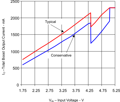 Figure 1. Maximum Total DC-DC Current vs Input Voltage
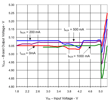 Figure 3. Boost Output Voltage vs Input Voltage
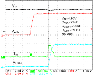 Figure 5. USB1 Start-Up After Enable – No Load
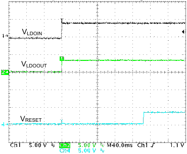
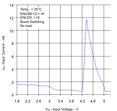 Figure 2. TPS2505 Typical On Input Current With No Load
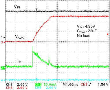
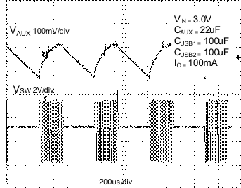 Figure 6. Boost Output Ripple in PFM Operation
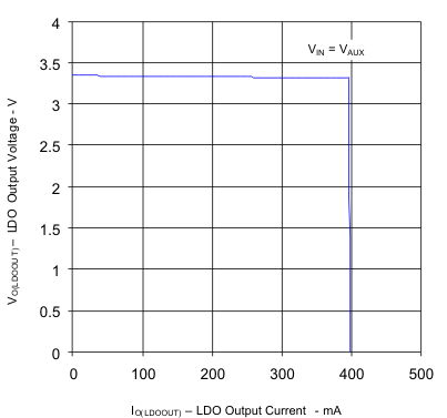 Figure 8. LDO Output Voltage vs Output Current