ZHCSP18A November 2021 – June 2022 TPS22953-Q1 , TPS22954-Q1
PRODUCTION DATA
- 1 特性
- 2 应用
- 3 说明
- 4 Revision History
- 5 Device Comparison Table
- 6 Pin Configuration and Functions
-
7 Specifications
- 7.1 Absolute Maximum Ratings
- 7.2 ESD Ratings
- Recommended Operating Conditions
- 7.3 Thermal Information
- 7.4 Electrical Characteristics
- 7.5 Electrical Characteristics – VBIAS = 5 V
- 7.6 Electrical Characteristics – VBIAS = 3.3 V
- 7.7 Electrical Characteristics – VBIAS = 2.5 V
- 7.8 Switching Characteristics – CT = 1000 pF
- 7.9 Switching Characteristics – CT = 0 pF
- 7.10 Typical DC Characteristics
- 7.11 Typical Switching Characteristics
- 8 Parameter Measurement Information
-
9 Detailed Description
- 9.1 Overview
- 9.2 Functional Block Diagram
- 9.3
Feature Description
- 9.3.1 On and Off Control (EN Pin)
- 9.3.2 Voltage Monitoring (SNS Pin)
- 9.3.3 Power Good (PG Pin)
- 9.3.4 Supervisor Fault Detection and Automatic Restart
- 9.3.5 Manual Restart
- 9.3.6 Thermal Shutdown
- 9.3.7 Reverse Current Blocking (TPS22953-Q1 Only)
- 9.3.8 Quick Output Discharge (QOD) (TPS22954-Q1 Only)
- 9.3.9 VIN and VBIAS Voltage Range
- 9.3.10 Adjustable Rise Time (CT Pin)
- 9.3.11 Power Sequencing
- 9.4 Device Functional Modes
- 10Application and Implementation
- 11Power Supply Recommendations
- 12Layout
- 13Device and Documentation Support
- 14Mechanical, Packaging, and Orderable Information
9.3.8 Quick Output Discharge (QOD) (TPS22954-Q1 Only)
The Quick Output Discharge (QOD) transistor is engaged indefinitely whenever the switch is disabled and the recommended VBIAS voltage is met. During this state, the QOD resistance (RPD) discharges VOUT to GND. TI does not recommend to apply a continuous DC voltage to OUT when the device is disabled.
The QOD transistor can remain active for a short period of time even after VBIAS loses power. This brief period of time is defined as tDIS. For best results, TI recommends the device get disabled before VBIAS goes below the minimum recommended voltage. The waveform in Figure 9-6 shows the behavior when power is applied and then removed in a typical application.
 Figure 9-6 Power Applied and Then
Removed in a Typical Application
Figure 9-6 Power Applied and Then
Removed in a Typical ApplicationAt the end of the tDIS time, it is not assured that VOUT is 0 V because the final voltage is dependent upon the initial voltage and the CL capacitor. The final VOUT can be calculated with Equation 3 for a given initial voltage and CL capacitor.
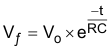
where
- Vf is the final VOUT voltage
- Vo is the initial VOUT voltage
- R is the the value of the output discharge resistor, RPD (see the Electrical Characteristics table)
- C is the output bulk capacitance on OUT