ZHCSP18A November 2021 – June 2022 TPS22953-Q1 , TPS22954-Q1
PRODUCTION DATA
- 1 特性
- 2 应用
- 3 说明
- 4 Revision History
- 5 Device Comparison Table
- 6 Pin Configuration and Functions
-
7 Specifications
- 7.1 Absolute Maximum Ratings
- 7.2 ESD Ratings
- Recommended Operating Conditions
- 7.3 Thermal Information
- 7.4 Electrical Characteristics
- 7.5 Electrical Characteristics – VBIAS = 5 V
- 7.6 Electrical Characteristics – VBIAS = 3.3 V
- 7.7 Electrical Characteristics – VBIAS = 2.5 V
- 7.8 Switching Characteristics – CT = 1000 pF
- 7.9 Switching Characteristics – CT = 0 pF
- 7.10 Typical DC Characteristics
- 7.11 Typical Switching Characteristics
- 8 Parameter Measurement Information
-
9 Detailed Description
- 9.1 Overview
- 9.2 Functional Block Diagram
- 9.3
Feature Description
- 9.3.1 On and Off Control (EN Pin)
- 9.3.2 Voltage Monitoring (SNS Pin)
- 9.3.3 Power Good (PG Pin)
- 9.3.4 Supervisor Fault Detection and Automatic Restart
- 9.3.5 Manual Restart
- 9.3.6 Thermal Shutdown
- 9.3.7 Reverse Current Blocking (TPS22953-Q1 Only)
- 9.3.8 Quick Output Discharge (QOD) (TPS22954-Q1 Only)
- 9.3.9 VIN and VBIAS Voltage Range
- 9.3.10 Adjustable Rise Time (CT Pin)
- 9.3.11 Power Sequencing
- 9.4 Device Functional Modes
- 10Application and Implementation
- 11Power Supply Recommendations
- 12Layout
- 13Device and Documentation Support
- 14Mechanical, Packaging, and Orderable Information
10.1.2 Thermal Considerations
The maximum IC junction temperature must be restricted to just under the thermal shutdown (TSD) limit of the device. Use Equation 6 to calculate the maximum allowable dissipation, PD(max) for a given output current and ambient temperature.
Equation 6. 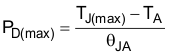
where
- PD(max) is the maximum allowable power dissipation.
- TJ(max) is the maximum allowable junction temperature before hitting thermal shutdown (see the Electrical Characteristics table).
- TA is the ambient temperature of the device.
- θJA is the junction to air thermal impedance. See the Thermal Information section. This parameter is highly dependent upon board layout.