ZHCS486A October 2011 – June 2015 TPS22933
PRODUCTION DATA.
6 Specifications
6.1 Absolute Maximum Ratings
over operating free-air temperature range (unless otherwise noted)(1)| MIN | MAX | UNIT | |||
|---|---|---|---|---|---|
| VIN | Input voltage | BAT, USB, DC_IN | –0.3 | 14 | V |
| VOUTPUT | Output voltage | VOUT, LOUT | –0.3 | 6 | V |
| VEN | Input voltage | EN | –0.3 | 6 | V |
| IMAX | Maximum continuous switch current | 75 | mA | ||
| IPLS | Maximum pulsed switch current, pulse <300 µs, 2% duty cycle | 100 | mA | ||
| TA | Operating free-air temperature | –40 | 85 | °C | |
| Tlead | Maximum lead temperature (10-s soldering time) | 300 | °C | ||
| Tstg | Storage temperature | –65 | 150 | °C | |
(1) Stresses beyond those listed under Absolute Maximum Ratings may cause permanent damage to the device. These are stress ratings only, which do not imply functional operation of the device at these or any other conditions beyond those indicated under Recommended Operating Conditions. Exposure to absolute-maximum-rated conditions for extended periods may affect device reliability.
6.2 ESD Ratings
| VALUE | UNIT | |||
|---|---|---|---|---|
| V(ESD) | Electrostatic discharge | Human-body model (HBM), per ANSI/ESDA/JEDEC JS-001(1) | ±2000 | V |
| Charged-device model (CDM), per JEDEC specification JESD22-C101(2) | ±1000 | |||
(1) JEDEC document JEP155 states that 500-V HBM allows safe manufacturing with a standard ESD control process. Manufacturing with less than 500-V HBM is possible with the necessary precautions. Pins listed as ±2000 V may actually have higher performance.
(2) JEDEC document JEP157 states that 250-V CDM allows safe manufacturing with a standard ESD control process. Manufacturing with less than 250-V CDM is possible with the necessary precautions. Pins listed as ±1000 V may actually have higher performance.
6.3 Recommended Operating Conditions
| MIN | NOM | MAX | UNIT | |||
|---|---|---|---|---|---|---|
| VIN | Input voltage | BAT, USB, DC_IN | 2.5 | 12 | V | |
| VEN | EN | 0 | 5.5 | V | ||
| VIH | EN pin High-level input voltage, (EN > VIH Min, VOUT = LDO Output) |
BAT = 2.5 V to 5.5 V, USB, DC_IN = 2.5 V to 12 V | 1.15 | 5.5 | V | |
| VIL | EN pin Low-level input voltage, (EN< VIL Max, VOUT = pulldown) |
BAT = 2.5 V to 5.5 V, USB, DC_IN = 2.5 V to 12 V | 0 | 0.6 | V | |
| IOUT-LOUT | LOUT Current | VBAT = 4.2 V OR VUSB = 5 V OR VDC_IN = 5 V, EN = 3.4 V, IOUT-VOUT = 0 mA |
50 | mA | ||
| IOUT-VOUT | VOUT Current | VBAT = 4.2 V OR VUSB = 5 V OR VDC_IN = 5 V, EN = 3.4 V, IOUT-LOUT = 0 mA |
50 | mA | ||
| IOUT-TOTAL | LOUT + VOUT current | VBAT = 4.2 V OR VUSB = 5 V OR VDC_IN = 5 V, EN = 3.4 V |
50 | mA | ||
| CAP | LDO Capacitor (on CAP pin) | 20(1) | nF | |||
| LOUT Capacitor | 1 | µF | ||||
| VOUT Capacitor | 1 | µF | ||||
(1) Refer to Application and Implementation.
6.4 Thermal Information
| THERMAL METRIC(1) | TPS22933 | UNIT | |
|---|---|---|---|
| RSE (UQFN) | |||
| 6 PINS | |||
| RθJA | Junction-to-ambient thermal resistance | 115.6 | °C/W |
| RθJC(top) | Junction-to-case (top) thermal resistance | 59.9 | °C/W |
| RθJB | Junction-to-board thermal resistance | 27.4 | °C/W |
| ψJT | Junction-to-top characterization parameter | 2.1 | °C/W |
| ψJB | Junction-to-board characterization parameter | 27.3 | °C/W |
| RθJC(bot) | Junction-to-case (bottom) thermal resistance | — | °C/W |
(1) For more information about traditional and new thermal metrics, see the Semiconductor and IC Package Thermal Metrics application report, SPRA953.
6.5 Electrical Characteristics
BAT = 2.5 V to 12.0 V, USB = 2.5 V to 12.0 V, DC_IN = 2.5 V to 12.0 V, TA = –40ºC to +85ºC (unless otherwise noted)| PARAMETER | TEST CONDITIONS(2) (3) (6) | TA | MIN | TYP(1) | MAX | UNIT | |
|---|---|---|---|---|---|---|---|
| IIN-BAT | Operating current | IOUT = 0 mA, VBAT = 4.2 V, VUSB = 3 V, VDC_IN = 3 V, EN = 3.4 V | Full | 9.2 | 15 | µA | |
| Quiescent current | IOUT = 0, VBAT = 4.2 V, VUSB = 5 V, VDC_IN = 3 V, EN = 3.4 V | 0.7 | 2 | ||||
| IIN-USB | Operating current | IOUT = 0 mA, VBAT = 4.2 V, VUSB = 5 V, VDC_IN = 3 V, EN = 3.4 V | Full | 9.2 | 15 | µA | |
| Quiescent current | IOUT = 0, VBAT = 4.2V, VUSB = 5V, VDC_IN = 5.5V, EN = 3.4 V | 0.7 | 2 | ||||
| IIN-DC_IN | Operating current | IOUT = 0 mA, VBAT = 4.2 V, VUSB = 3 V, VDC_IN = 5 V, EN = 3.4 V | Full | 9.2 | 15 | µA | |
| Quiescent current | IOUT = 0, VBAT = 4.2V, VUSB = 5.5V, VDC_IN = 5V, EN = 3.4 V | 0.7 | 2 | ||||
| IIN-USB | Hi-Voltage operating current | IOUT = 0 mA, VBAT = 4.2 V, VUSB = 12 V, VDC_IN = 5 V, EN = 3.4 V | Full | 10.8 | 20 | µA | |
| IIN-DC_IN | Hi-Voltage operating current | IOUT = 0 mA, VBAT = 4.2 V, VUSB = 5 V, VDC_IN = 12 V, EN = 3.4 V | Full | 10.8 | 20 | µA | |
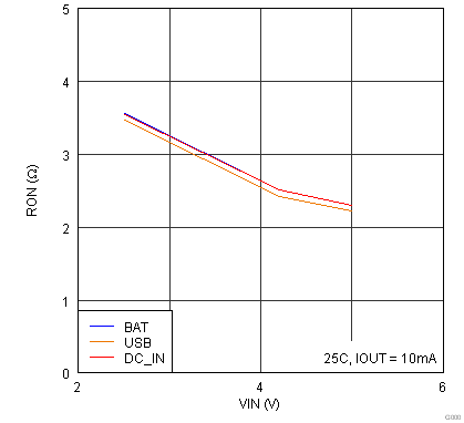
| RON | ON resistance (USB to CAP, BAT to CAP, DC_IN to CAP) | VIN = 5.0 V, IOUT = 10 mA | 25ºC | 2.4 | 3.3 | Ω | |
| Full | 3.5 | ||||||
| VIN = 4.2 V, IOUT = 10 mA | 25ºC | 2.6 | 3.5 | Ω | |||
| Full | 4 | ||||||
| VIN = 2.5 V, IOUT = 10 mA | 25ºC | 3.8 | 5 | Ω | |||
| Full | 6 | ||||||
| RONVOUT | ON resistance (LDO output to VOUT) | VIN = 4.2 V, IOUT-VOUT = 10 mA | 25ºC | 1.3 | 2.5 | Ω | |
| Full | 3 | ||||||
| RPD | Output pulldown resistance | VIN = 4.2 V, VEN = 0 V, I(into VOUT) = 10 mA | 25ºC | 63.8 | 120 | Ω | |
| IEN | EN input leakage | VEN = 1.6 V to 5.5 V or GND | Full | 1 | µA | ||
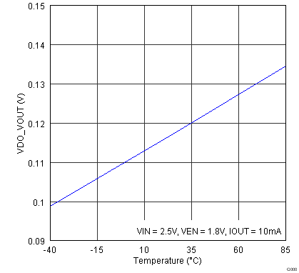
| VDO-VOUT | Dropout voltage VOUT (4) (5) | IOUT = 10 mA | Full | 0.11 | V | ||
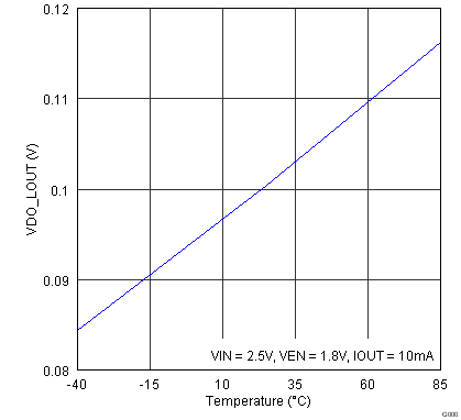
| VDO-LOUT | Dropout voltage LOUT | IOUT = 10 mA(4) (5) | Full | 0.1 | V | ||
| VLOUT | Always on LDO output voltage (LOUT pin) | VIN < 3.4 V, IOUT = 10 mA, VEN = 1.8 V | Full | VIN – VDO-LOUT | V | ||
| VIN > 4 V, IOUT = 10 mA, VEN = 1.8 V | Full | 3.42 | 3.6 | 3.78 | |||
| VVOUT | Switched LDO output voltage (VOUT pin) | VIN < 3.4 V, IOUT = 10 m A, VEN = 1.8 V | Full | VIN – VDO-VOUT | V | ||
| VIN > 4 V, IOUT = 10 mA, VEN = 1.8 V | Full | 3.39 | 3.57 | 3.75 | |||
| VCO | Changeover voltage | VBAT = 4.2 V, VUSB = 4.0 V rising to 4.4 V | Full | 0.15 | V | ||
| tCO | Changeover time | VBAT=4.2 V, VUSB = 4.0 V rising to 4.4 V, CAP = 0.01 µF, IOUT = 10 mA | 25ºC | 18 | µs | ||
| Full | 50 | ||||||
| tOFF | VOUT OFF-time | EN high to low, C(VOUT) = 1 µF, VOUT load = 360 Ω | Full | 32 | µs | ||
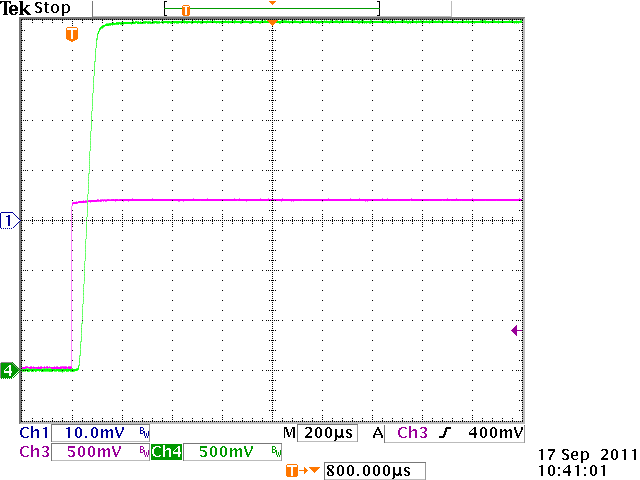
| tON | VOUT ON-time | EN low to high, C(VOUT) = open, VOUT load = 360 Ω | Full | 65 | µs | ||
(1) TYP is 25ºC, BAT = 4.2-V, USB = 0-V, DC_IN = 0-V.
(2) VIN is defined as the highest voltage present on the BAT, USB and DC_IN pins.
(3) One of the voltages on BAT, USB and DC_IN must be > VIN (Min), others can be 0 V.
(4) Dropout voltage is the minimum input to output voltage differential needed to maintain regulation at a specified output current. In dropout, the output voltage is equal to: VIN – VDROPOUT.
(5) Dropout voltage is measured at the VIN that causes the output to drop to 100mV below its nominal voltage. For VOUT, the voltage drop across the output switch is included (10mA × RONVOUT).
(6) VBAT, VUSB and VDC_IN refer to the voltages on BAT, USB and DC_IN respectively. OUT, IOUT-VOUT and IOUT-LOUT refer to the currents for the combined output current for VOUT and LOUT, the current on VOUT and the current on LOUT respectively.
6.6 Typical Characteristics
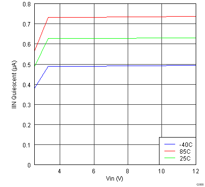
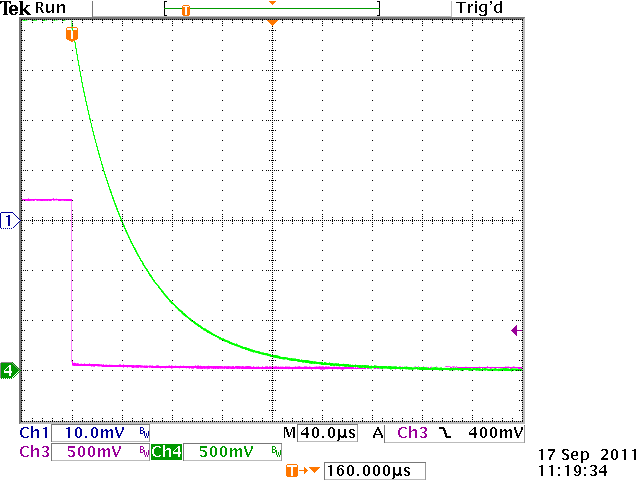
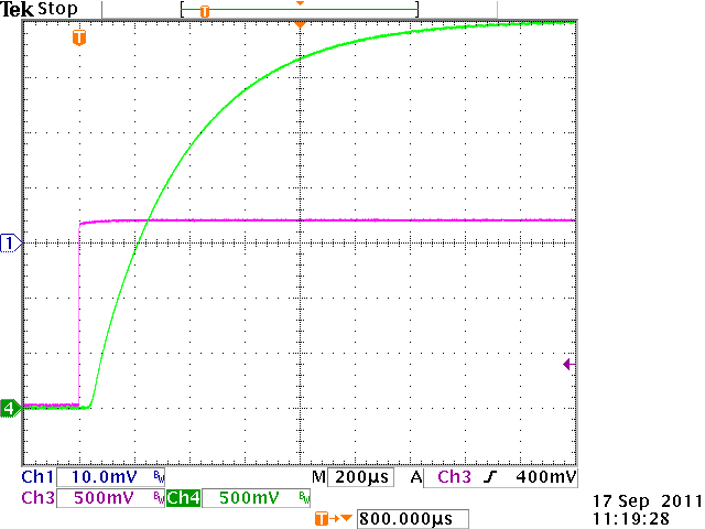
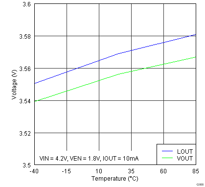
Table 1. Performance Graphs and Plots
| Type | Description | Figure |
|---|---|---|
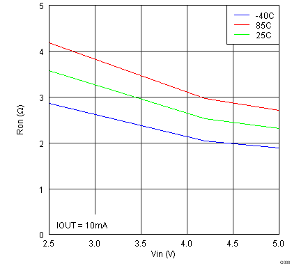
| Graph | RON versus VIN (BAT, USB, DC_IN) 25°C | Figure 1 |
| Graph | RON versus VIN (Any input) | Figure 2 |
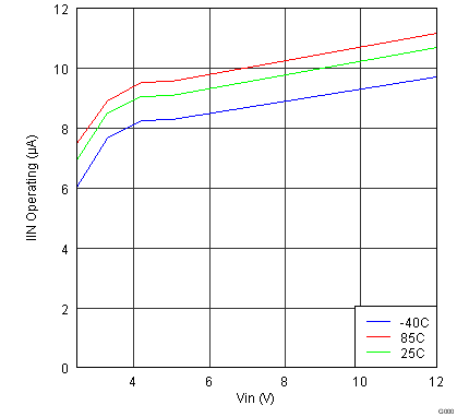
| Graph | Quiescent Current versus Input Voltage (Any input) | Figure 3 |
| Graph | Operating Current versus Input Voltage (Any Input) | Figure 4 |
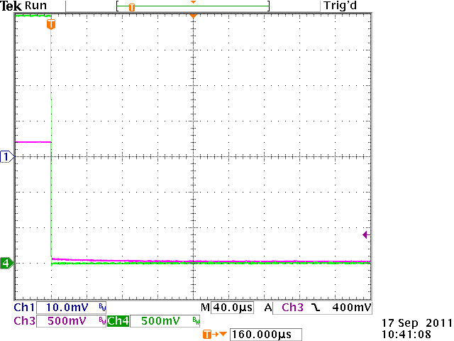
| Scope Plot | tOFF (VIN = 4.2 V, C(VOUT) = 1 uF, 25°C) | Figure 5 |
| Scope Plot | tOFF (VIN = 4.2 V, C(VOUT) = open, 25°C) | Figure 6 |
| Scope Plot | tON (VIN = 4.2 V, C(VOUT) = 1 uF, 25°C) | Figure 7 |
| Scope Plot | tON (VIN = 4.2 V, C(VOUT) = open, 25°C) | Figure 8 |
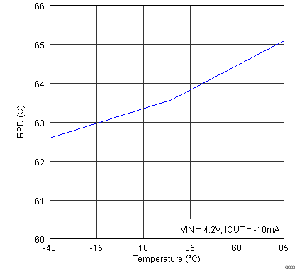
| Graph | LOUT and VOUT versus Temperature at VIN = 4.2 V | Figure 9 |
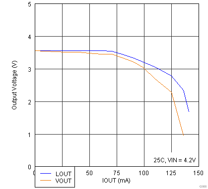
| Graph | LOUT and VOUT versus IOUT (VIN = 4.2 V, Temp = 25°C) | Figure 10 |
| Graph | LOUT Dropout Voltage versus Temperature (VIN = 2.5 V) | Figure 11 |
| Graph | VOUT Dropout Voltage versus Temperature (VIN = 2.5 V) | Figure 12 |
| Graph | Output Pulldown Resistance (RPD) versus Temperature (10 mA into VOUT) | Figure 13 |
