ZHCS486A October 2011 – June 2015 TPS22933
PRODUCTION DATA.
9 Application and Implementation
NOTE
Information in the following applications sections is not part of the TI component specification, and TI does not warrant its accuracy or completeness. TI’s customers are responsible for determining suitability of components for their purposes. Customers should validate and test their design implementation to confirm system functionality.
9.1 Application Information
9.1.1 LDO Capacitor (for CAP Pin)
An optional capacitor on the CAP pin helps stabilize the integrated LDO. Take care in capacitor sizing to reduce inrush currents. The voltage on the CAP pin will follow the highest input. Since the max input voltage is 12 V, the capacitor voltage rating must be higher than 12 V.
9.1.2 Using the CAP Pin as a Power Output
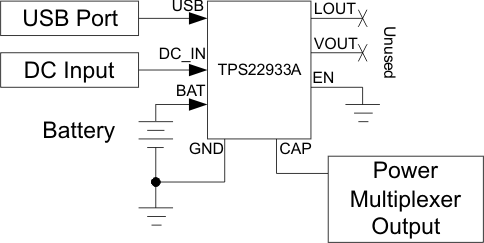
Figure 17 shows three power inputs multiplexed to source only through the CAP pin. In this case, the LDO outputs are not used (EN is tied low). The highest of the inputs is chosen to drive the voltage at the CAP pin.
 Figure 17. Using the CAP Pin as a Multiplexer Output
9.2 Typical Application
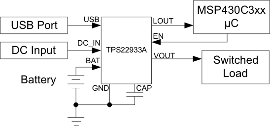
Figure 18 shows three power inputs multiplexed to source the LDO. The LDO always on output (LOUT) is tied to an MSP430. The MSP430 then determines when to enable the switched output (VOUT) by driving the EN pin.
 Figure 18. Application Example
9.2.1 Design Requirements
Table 4 lists the design parameters for TPS22933.
Table 4. Design Parameters
| INPUT | VOLTAGE | |
|---|---|---|
| USB Port | 5.0V | |
| DC Input | 5.0V | |
| Battery | 4.2V | |
9.2.2 Detailed Design Procedure
Initial power up:
DC_IN = 0 V; USB = 0 V; EN = 0 V
BAT is applied at 4.2 V
LDO power comes from BAT
LOUT = 3.6 V; CAP = 4.2 V; VOUT = 0 V
USB power is connected at 5 V, BAT remains 4.2 V and DC_IN remains 0 V
LDO power is changed from BAT to USB in tCO
LOUT = 3.6 V; CAP = 5 V; VOUT = 0 V
DC_IN power is connected at 5.0 V, BAT remains 4.2 V and USB remains 5 V
No change in LDO power
LOUT = 3.6 V; CAP = 5 V; VOUT = 0 V
EN = VIH, BAT remains 4.2 V, USB remains 5 V and DC_IN remains 5 V
LOUT = 3.6 V, CAP = 5 V; VOUT = 3.6 V
USB power is removed, BAT remains 4.2 V and DC_IN remains 5 V
LDO power is changed from USB to DC_IN
LOUT = 3.6 V; CAP = 5 V; VOUT = 3.6 V
DC_IN power is removed, BAT remains 4.2 V and USB remains 0 V:
LDO power is changed from DC_IN to BAT
LOUT = 3.6 V; CAP = 4.2 V; VOUT = 3.6 V
9.2.3 Application Curve
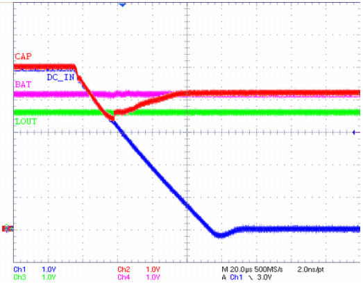
Figure 19 shows the device behavior in the last step of the design procedure, when DC_IN power is removed and the LDO is powered by the battery. The capacitor on the CAP pin discharges as DC_IN is removed but then charges to the battery voltage when the input is automatically switched. LOUT remains a constant 3.6 V throughout this power switching.
 Figure 19. DC_IN Removed, BAT Powers LDO (LOUT = 3.6 V)