ZHCSHN4D February 2018 – September 2021 TPS1H200A-Q1
PRODUCTION DATA
- 1 特性
- 2 应用
- 3 说明
- 4 Revision History
- 5 Pin Configuration and Functions
- 6 Specifications
- 7 Detailed Description
- 8 Application and Implementation
- 9 Power Supply Recommendations
- 10Layout
- 11Device and Documentation Support
- 12Mechanical, Packaging, and Orderable Information
7.3.2.2 Latch-Off Mode
Latch-off mode is active when the DELAY pin connects to GND through a capacitor. When a current limit is reached, the output current holds at the setting current, but latches off after a preset DELAY time (tdl1+ tdl2). tdl1 is the default delay time, and tdl2 is a configurable delay time set by a capacitor. Regardless of whether the current limit is removed or not, the output remains latched off. The output only recovers when IN is toggling.
tdl2 can be calculated by Equation 2.
Equation 2. 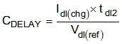
where
- CDELAY is the capacitor connected on the DELAY pin.
- The Idl(chg) is the device that charges the current in latch-off mode.
- tdl2 is the user-setting delay time.
- Vdl(ref) is the internal reference voltage in latch-off mode.
 Figure 7-4 Latch-Off-Mode Connection
 Figure 7-5 Latch-Off-Mode Example