ZHCSDD8D October 2014 – December 2019 TPS1H100-Q1
PRODUCTION DATA.
- 1 特性
- 2 应用
- 3 说明
- 4 修订历史记录
- 5 Pin Configuration and Functions
- 6 Specifications
-
7 Detailed Description
- 7.1 Overview
- 7.2 Functional Block Diagram
- 7.3
Feature Description
- 7.3.1 Accurate Current Sense
- 7.3.2 Programmable Current Limit
- 7.3.3 Inductive-Load Switching-Off Clamp
- 7.3.4
Full Protections and Diagnostics
- 7.3.4.1 Short-to-GND and Overload Detection
- 7.3.4.2 Open-Load Detection
- 7.3.4.3 Short-to-Battery Detection
- 7.3.4.4 Reverse-Polarity Detection
- 7.3.4.5 Thermal Protection Behavior
- 7.3.4.6 UVLO Protection
- 7.3.4.7 Loss of GND Protection
- 7.3.4.8 Loss of Power Supply Protection
- 7.3.4.9 Reverse Current Protection
- 7.3.4.10 Protection for MCU I/Os
- 7.3.5 Diagnostic Enable Function
- 7.4 Device Functional Modes
- 8 Application and Implementation
- 9 Power Supply Recommendations
- 10Layout
- 11器件和文档支持
- 12机械、封装和可订购信息
7.3.1 Accurate Current Sense
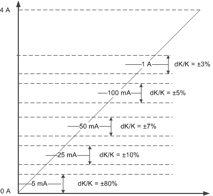
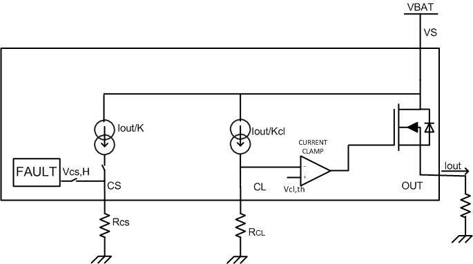
For version B, the high-accuracy current-sense function is internally implemented, which allows a better real-time monitoring effect and more-accurate diagnostics without further calibration. A current mirror is used to source 1 / K of the load current, flowing out to the external resistor between the CS pin and GND, and reflected as voltage on the CS pin.
K is the ratio of the output current and the sense current. It is a constant value across the temperature and supply voltage. Each device was internally calibrated while in production, so post-calibration by users is not required in most cases.
 Figure 29. Current-Sense Accuracy
 Ensure the CS voltage is in the linear region (0 to 4 V) during normal operation. Calculate RCS with Equation 1.

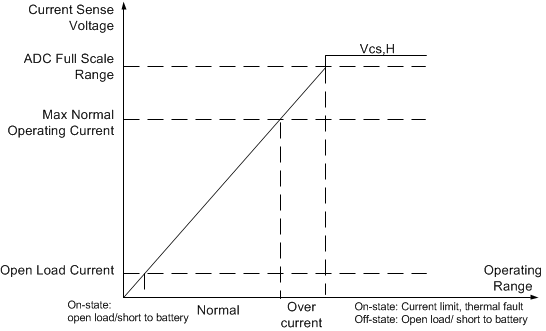
Also, when a fault condition occurs, CS works as a diagnostics report pin. When an open load or short to battery occurs in the on-state, VCS almost equals 0. When current limit, thermal shutdown/swing, open load, or short to battery in the off-state occurs, the voltage is pulled up to VCS,h. Figure 30 shows a typical current-sense voltage according to the operating conditions, including fault conditions.
 Figure 30. Voltage Indication on the Current-Sense Pin
  Figure 31. Current-Sense and Current-Limit Block Diagram