SLDS182A August 2010 – July 2015 TPIC7218-Q1
PRODUCTION DATA.
- 1 Device Overview
- 2 Revision History
- 3 Pin Configuration and Functions
-
4 Specifications
- 4.1 Absolute Maximum Ratings
- 4.2 ESD Ratings
- 4.3 Recommended Operating Conditions
- 4.4 Thermal Information
- 4.5 Input Port Electrical Characteristics
- 4.6 PWM Low-Side Driver Electrical Characteristics
- 4.7 Digital Low-Side Driver Electrical Characteristics
- 4.8 High-Side Driver Electrical Characteristics
- 4.9 K-Line Electrical Characteristics
- 4.10 Warning Lamp Electrical Characteristics
- 4.11 Power Supply Electrical Characteristics
- 4.12 SPI Electrical Characteristics
- 4.13 WL_LS Low-Side Switch Output Characteristics
- 4.14 Wheel-Speed High-Side Driver Characteristics
- 4.15 Wheel-Speed Low-Side Driver Characteristics
- 4.16 Wheel-Speed Output Characteristics
- 4.17 RST Output Characteristics
- 4.18 SPI Timing Electrical Characteristics
- 4.19 Power Supply Switching Characteristics
- 4.20 Wheel-Speed Counter Switching Characteristics
- 4.21 HS Driver Switching Characteristics
- 4.22 Digital Low-Side Driver Switching Characteristics
- 4.23 PWM Low-Side Driver Switching Characteristics
- 4.24 K-Line Switching Characteristics
- 4.25 Warning Lamp Switching Characteristics
- 4.26 Watchdog Switching Characteristics
- 4.27 Wheel Speed Interface Switching Characteristics
- 4.28 Wheel-Speed High-Side Driver Switching Characteristics
- 4.29 Wheel-Speed Output Switching Characteristics
- 4.30 Typical Characteristics
-
5 Detailed Description
- 5.1 Overview
- 5.2 Functional Block Diagram
- 5.3
Feature Description
- 5.3.1 Ground Connections
- 5.3.2 Charge Pump
- 5.3.3 Reference Current Generator
- 5.3.4 Wheel-Speed Reference, VREF
- 5.3.5 Faults Common To Most Functional Blocks
- 5.3.6 PWM Low-Side Drivers
- 5.3.7 Digital Low-Side Drivers
- 5.3.8 High-Side Drivers
- 5.3.9 Wheel-Speed Sensing
- 5.3.10 K-Line
- 5.3.11 Warning Lamp Drivers
- 5.3.12 Watchdog Operation
- 5.4 Device Functional Modes
- 5.5 Programming
- 5.6 Register Maps
- 6 Application and Implementation
- 7 Power Supply Recommendations
-
8 Layout
- 8.1
Layout Guidelines
- 8.1.1 Local Grounding Configuration
- 8.1.2 Board Level Grounding Configuration, TPIC7218-Q1 to System Connector
- 8.1.3 VCC3 Bypass Capacitor
- 8.1.4 VDD Bypass Capacitor
- 8.1.5 VBAT and CHP Capacitors
- 8.1.6 Multiple Plane Layer Assignments
- 8.1.7 Duplicate Pad Under TPIC7218-Q1 on All Non-Ground Plane Inner Layers
- 8.1.8 Flooding
- 8.2 Layout Example
- 8.1
Layout Guidelines
- 9 Device and Documentation Support
- 10Mechanical, Packaging, and Orderable Information
5 Detailed Description
5.1 Overview
The TPIC7218-Q1 device is an anti-lock braking controller capable of directly driving eight solenoid valves with internal high-current low-side drivers. Low-side drivers configured for digital control do not require external voltage clamps. The TPIC7218-Q1 device has gate drive capability for two high-side N-Channel MOSFETs that can be used to drive a pump motor and power to all solenoids. The TPIC7218-Q1 device provides a fault-tolerant interface for both Intelligent and Active wheel-speed sensors to an external microprocessor.
The TPIC7218-Q1 device can be used with either 3.3- or 5-V microprocessors and uses a standard SPI (Serial-Peripheral Interface). The TPIC7218-Q1 device has two internal open-drain warning lamp drivers that can be pulled up to battery voltage, as well as one low-voltage driver. An internal state machine monitors a watchdog input and reports faults on a warning-lamp pin and SPI register. A K-Line transceiver is also included. A multitude of safety and fault monitoring functionality supervise both system and TPIC7218-Q1 circuits. Faults must be polled and reset over SPI.
The TPIC7218-Q1 device is designed for use in harsh automotive environments, capable of withstanding high operating temperatures and electrically noisy signals and power. Short-to-ground, short-to-battery, and open-load conditions are tolerated and monitored. The TPIC7218-Q1 device also exhibits outstanding electromagnetic compatibility (EMC) performance.
5.2 Functional Block Diagram
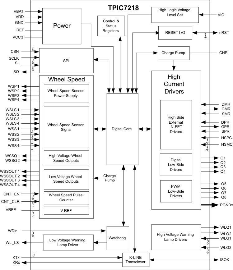
5.3 Feature Description
5.3.1 Ground Connections
The TPIC7218-Q1 device has two types of grounds: Power-grounds (PGND), which are used to provide a path for internal high-current open-drain FETs, and ground (GND), which are used to provide ground to all analog and digital circuitry. All the PGND pins and the thermal pad are internally shorted together. A very-low impedance connection exists internal to the TPIC7218-Q1 device between all power grounds and the ground pin (pin 6). TI recommends that all PGND, GND, and PowerPad pins be connected together at the pins of the TPIC7218-Q1 device to a solid ground plane. Failure to implement the grounding in this way is likely to result in poor EMC performance.
5.3.2 Charge Pump
An internal charge pump generates the charge necessary for proper operation of all drivers. A capacitor with a value of 100 nF connected between the CHP pin and VBAT pin is required for proper operation. The voltage on the CHP pin is typically 12 V greater than the voltage on the VBAT pin. When selecting a charge pump capacitor, care must be taken to ensure that the capacitors specifications are not violated.
5.3.3 Reference Current Generator
The TPIC7218-Q1 device generates an internal reference current that is output on the REF pin. This pin requires a 10-kΩ, ±1% resistor connected to GND.
5.3.4 Wheel-Speed Reference, VREF
The voltage set on the VREF pin must be stable at all times. If this voltage deviates from the desired setting, then all the wheel-speed thresholds will change. TI recommends externally monitoring the VREF voltage to ensure proper operation of the wheel-speed functional block.
5.3.5 Faults Common To Most Functional Blocks
Table 5-1 Summary Fault State Table
| EVENT | GMR | GPR | WLQ1 | WLQ2 | WL_LS | nRST | Q1-Q4 | Q5-Q8 | WSPx | WSLSx | SPI |
|---|---|---|---|---|---|---|---|---|---|---|---|
| VDD undervoltage shutdown | OFF | OFF | High Z | High Z | Low | Low | High Z | High Z | OFF | High Z | YES(1) |
| VDD undervoltage reset | OFF | OFF | High Z | High Z | High Z | High Z | High Z | High Z | OFF | High Z | NO |
| Recovery after VDD undervoltage reset (VDD>4.85V) | OFF | OFF | High Z | High Z | Low | High Z | High Z | High Z | OFF | High Z | YES |
| Recovery after VDD undervoltage reset (VDD<4.75V) | OFF | OFF | High Z | High Z | Low | Low | High Z | high Z | OFF | High Z | YES |
| VBAT overvoltage | Not affected(2) | ON | Not affected | Not affected | Not affected | Not affected | High Z | High Z | OFF | High Z | YES |
| VBAT undervoltage | OFF | OFF | Not affected | Not affected | Not affected | Not affected | High Z | High Z | Not affected | Not affected | YES |
| Thermal fault (OTSD = ‘1’) |
Not affected | Not affected | High Z(4) | High Z | Not affected | Not affected | High Z | High Z | Not affected | Not affected | YES |
| Watchdog bad (WDSTAT =’0’) | OFF | OFF | High Z | High Z | Low | High Z | High Z | High Z | Not affected | Not affected | YES |
| While in Reset because of Watchdog going to state ‘000’ | OFF | OFF | High Z | High Z | Low | Low | High Z | High Z | OFF | High Z | YES(3) |
| external reset by pulling nRST pin low | OFF | OFF | High Z | High Z | Low(5) | Low | High Z | High Z | OFF | High Z | YES(1) |
5.3.6 PWM Low-Side Drivers
The TPIC7218-Q1 device features eight low-side drivers, four of which can be used for pulse width modulation (PWM) of solenoids. The low-side driver pins: Q5, Q6, Q7, and Q8 are open-drain MOSFETs that are capable of sinking large amounts of current. Each driver is monitored for three fault conditions: overcurrent, open-load, and over-temperature. In addition, driver operation is dependent on other fault conditions: VBAT undervoltage, VBAT overvoltage, VDD undervoltage, watchdog fault. See the application circuit and register diagram in Figure 5-1.
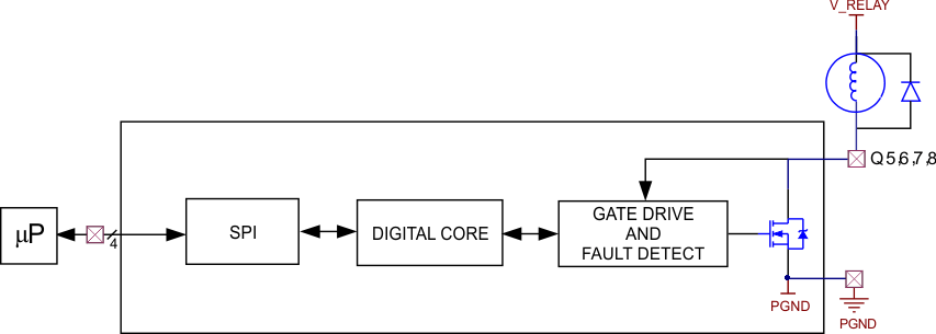 Figure 5-1 PWM Driver Register and Application Circuit Diagram
Each PWM driver features a 10-bit configurable duty-cycle setting, and options for independent phase control. Available phases of 0°, 90°, 180°, and 270° can be set for each driver in registers 0x14, 0x16, 0x18, and 0x1A. Changes in the dedicated 2-bits result in a phase change in the following complete period to prevent glitches. Table 5-2 lists the available phase options based on the settings of the dedicated 2-bit selection
Table 5-2 PWM Phase Selection
| PWMQXPhase<1> | PWMQXPhase<0> | SELECTED PHASE |
|---|---|---|
| 0 | 0 | 0° |
| 1 | 0 | 90° |
| 0 | 1 | 180° |
| 1 | 1 | 270° |
Each duty cycle of the PWM driver can be selected by setting the appropriate bits using Equation 1.

For example, a setting of 0x3FF causes a 100% duty cycle and a setting of 0x000 causes a 0% duty cycle.
All 10 bits must be written for the new duty cycle code to be latched into the state machine. Changes in the 10-bit result in a duty-cycle change in the following complete period to prevent glitches. PWM drivers can be used as digital drivers by fully turning them on (100% duty cycle) and off (0% duty cycle). However, care must be taken not to violate electrical specifications when using PWM drivers in this way (such as energy handling capability).
The frequency is also configurable (see Table 5-3), but is not independent for each enabled driver; all PWM drivers are set by selecting a 2-bit value in register 0x12. Frequency selection changes take place only when the PWM drivers are disabled and then re-enabled.
Table 5-3 PWM Frequency Selection
| PWMFreq<1> | PWMFreq<0> | SELECTED FREQUENCY |
|---|---|---|
| 0 | 0 | 2 kHz |
| 1 | 0 | 4 kHz |
| 0 | 1 | 8 kHz |
| 1 | 1 | 16 kHz |
For example, if Q5 is enabled while the frequency setting is <00> but Q6 is enabled after the frequency setting was changed to <11>, then Q5 is switching at 2 kHz and Q6 is switching at 16 kHz.
Each PWM driver monitors, reports, and has integrated protection for many electrical fault conditions. Overcurrent faults are reported as a 1 in register 0x02, (bits 0, 2, 4, and 6 are referenced by bits F5, F6, F7, and F8) and cause the affected driver to disable after a deglitch time of toff_blank_PWMx. Over-temperature (junction) faults are reported in register 0x03, (bit-6 OTSD) and cause not only the affected driver, but also the adjacent driver to disable after a deglitch time of toff_tmp_PWMx. The PWM drivers also check for an open-load or short to ground condition whenever they are not disabled. This type of fault is reported as 1 in register 0x02, (bits 1, 3, 5, 7 are referenced by bits S5, S6, S7, and S8). A master low-side fault bit in register 0x00, (bit-0) becomes high whenever any of the previously mentioned overcurrent or open-load faults occur. Fault flags can be cleared after the removal of the fault condition by reading the appropriate fault reporting register. When the fault flags are cleared, the low-side master fault bit (FAIL) can be cleared by reading it.
The PWM drivers also respond to fault conditions within other functional blocks. The drivers are disabled whenever VBAT undervoltage, VBAT overvoltage, or VDD undervoltage fault bits in register 0x00 are set. Also watchdog fault can cause PWM drivers to disable, if register 0x11, bit-4 (WD_EN) is set. This bit defaults to 0 upon power up. Any of these faults do not cause the FAIL bit to be set.
Faults can be cleared by reading the appropriate fault reporting register. When the faults are cleared, the drivers can be re-enabled. To enable or re-enable a driver, simply toggle the driver bits (GE5, GE6, GE7, GE8) by writing a 0, then 1. Fault reporting bits do not have any affect on PWM drivers; only the actual fault condition causes a driver to disable. Nevertheless, TI recommends clearing the fault bits by reading these bits before enabling the drivers.
Besides monitoring and reporting faults, PWM drivers have overvoltage-protection circuitry built in. An active-clamp monitors the voltage on PWM driver pins and limits it to Vcl_PWMx. At the system level, PWM drivers use an external recirculation diode in parallel with the inductive load.
5.3.7 Digital Low-Side Drivers
The TPIC7218-Q1 device features eight low-side drivers, four of which can be used digital control of solenoids. The low-side driver pins: Q1, Q2, Q3, and Q4 are open-drain MOSFETs that are capable of sinking large amounts of current. Each driver is monitored for three fault conditions: overcurrent, open-load, and over-temperature. However, driver operation also is dependant on other fault conditions: VBAT undervoltage, VBAT overvoltage, VDD undervoltage, watchdog fault. See the application circuit and register diagram in Figure 5-2.
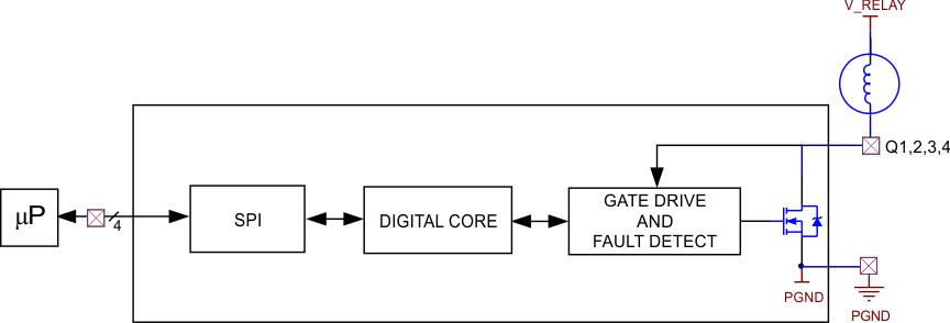 Figure 5-2 Digital Driver Register and Application Circuit Diagram
Each digital driver monitors, reports, and has integrated protection for many electrical fault conditions. Overcurrent faults are reported as a 1 in register 0x01, (bits 0, 2, 4, and 6 are referenced by bits F1, F2, F3, and F4) and cause the affected driver to disable after a deglitch time of toff_blank_DLSx. Over-temperature (junction) faults are reported in register 0x03, (bit-6 OTSD) and cause not only the affected driver, but also the adjacent driver to disable after a deglitch time of toff_tmp_DLSLx. Digital drivers also check for an open-load or short to ground condition whenever they are not enabled. This type of fault is reported as a 1 in register 0x01, (bits 1, 3, 5, 7 are referenced by S1, S2, S3, and S4). The master low-side fault bit in register 0x00, (bit-0) becomes high whenever an overcurrent or open-load fault occurs. Fault flags can be cleared after the removal of the fault condition by reading the appropriate fault reporting register. When this occurs the low-side master fault bit (FAIL) can be cleared by reading it.
The digital drivers also respond to fault conditions within other functional blocks. These drvers are disabled whenever the VBAT undervoltage, VBAT overvoltage, or VDD undervoltage fault bits in register 0x00 are set. Also, a watchdog fault can cause the digital drivers to disable if register 0x11, bit-4 (WD_EN) is set. This bit defaults to 0 upon power up. Any of these faults do not cause the FAIL bit to be set.
Faults can be cleared by reading the appropriate fault reporting register. When this is complete the digital drivers can be re-enabled. To enable or re-enable a driver, simply toggle the driver bits (GE1, GE2, GE3, GE4) by writing a 0, then 1. Fault reporting bits do not have any affect on the digital drivers; only the actual fault condition will cause a driver to disable. Nevertheless, TI recommends clearing the fault bits by reading them before enabling the drivers.
Besides monitoring and reporting faults, digital drivers have overvoltage protection circuitry built in. An active-clamp monitors voltage on the pins of these drivers and limits the voltage to Vcl_DLSx.
5.3.8 High-Side Drivers
The TPIC7218-Q1 device features two independent high-side gate drivers to control and monitor external N-Channel FETs. The pins, GPR, SPR, and DPR, are typically used to control an external N-MOSFET for the purpose of providing power to a motor pump. The pins, GMR, SMR, and DMR are typically used to control an external N-MOSFET for the purpose of providing power to the solenoid coils. When activated, the gate voltage drive on the GPR and GMR pins is sufficient to provide a strong VGS because of a built-in charge pump. High-side drivers are electrically protected and monitored for fault conditions.
5.3.8.1 High-Side Terminals: GPR, SPR, DPR, and HSPC
The GPR, SPR, and DPR (gate, source, and drain-pump relay) pins connect to an external N-MOSFET as shown in Figure 5-3. The purpose of this MOSFET is to relay the VBAT power to a pump motor. The N-MOSFET is turned on when the GPR pin is enabled. The GPR pin is controlled by either the HSPC pin or the GE_PR bit, bit-3 of address 0x11 as listed in Table 5-4.
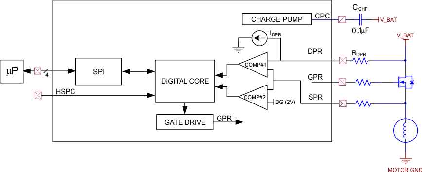 Figure 5-3 GPR, SPR, DPR, and HSPC Register and Application Circuit Diagram
Table 5-4 High-Side Operation Logic
| HSPC PIN | GE_PR BIT | GPR GATE PIN |
|---|---|---|
| LOW | 0 | OFF |
| LOW | 1 | ON |
| HIGH | 0 | ON |
| HIGH | 1 | ON |
| OPEN | 1 | ON |
| OPEN | 0 | OFF |
The overcurrent detection of the external N-MOSFET is triggered by a voltage difference between the DPR and SPR pins in comparator COMP #1. To set the overcurrent threshold the external series resistor, RDPR, must be sized to generate a particular input voltage (in conjunction with IDPR) on one input of the comparator. The other input voltage of the comparator changes as a function of the RDSON(MAX) and IDS values of the N-MOSFET. By comparing these voltages, the N-MOSFET overcurrent condition is reported. Given the RDSON(MAX) value of the N-MOSFET and the desired overcurrent threshold, RDPR can be calculated using Equation 2.

If the VDS value of the N-MOSFET exceeds the threshold set by the comparator for more than the deglitcher time, tOCdet, the GPR pin switches off and the appropriate fault flag (OCPR) is set high. When the overcurrent condition ends, the GPR pin can be switched on again with the SPI enable bit or the external enable pin.
Faults detected on VDD, VBAT, Watchdog (if WD_EN bit is high) prevent the high-side driver from enabling; GPR remains low or turns off. At the time the high-side driver is enabled, voltage on GPR pin is tested for a short-to-ground condition only after a certain delay time defined as tSTGPR. If a short is detected the GPR pin remains low. Any time the high-side driver is enabled overcurrent in the external MOSFET, short-to-ground on GPR, and short-to-ground on SMR can cause a fault condition and disable the high-side driver.
An overvoltage condition (such as load-dump) on VBAT turns the GPR pin on (clamping any energy from the alternator). If VBAT returns to normal operating voltage from an overvoltage fault condition, the GPR pin remains on for a minimum time, tGPRact.
If an overvoltage condition occurs on VBAT, the fault flag, FOV, is set after a deglitch time, tFovdet. With the overvoltage removed, the FOV flag can be cleared by reading address 0x00. After the fault bit is cleared, the GPR pin can be re-enabled. The GPR pin does not respond to successive overvoltage conditions until after a blanking time. See Table 5-5 and Figure 5-4 for more details.
Table 5-5 Pump Relay Fault and Operation
| SYSTEM EVENT | FAULT BITS AFFECTED | TPIC7218-Q1 STATE | NOTES | |
|---|---|---|---|---|
| BEFORE EVENT | AFTER EVENT | |||
| VDD Undervoltage | PORn = 1 | GPR ON | GPR OFF | nRST is internally driven low |
| VBAT Overvoltage (>VovVBAT) | FOV = 1 | GPR OFF | GPR ON | |
| VBAT Undervoltage (<VuvVBAT) | FUV = 1 | GPR ON | GPR OFF | |
| Watchdog fault ( must be enabled) | WDSTAT = 0, WD_FAULT = 1 | GPR ON | GPR OFF | WD_EN = 1 (enabled) |
| nRST pin externally driven low | Erst = 1 | GPR ON | GPR OFF | |
| Overcurrent in motor | OCPR=1,FHSD = 1 | GPR ON | GPR OFF | OCPRDIS = 0 (disabled) |
| Overcurrent in motor | OCPR=1,FHSD = 1 | GPR ON | GPR ON | OCPRDIS = 1 (enabled) |
| Short to GND on GPR, while GPR is OFF (time > tSTGPR) | FGPR = 1,FHSD = 1 | GPR OFF | GPR OFF | FGPRDIS = 0 (disabled), turn ON GPR |
| Short to GND on GPR, while GPR is ON | FGPR = 1,FHSD = 1 | GPR ON | GPR OFF | FGPRDIS = 0 (enabled) |
| Short to GND on GPR, while GPR is OFF (time > tSTGPR) | FGPR = 1,FHSD = 1 | GPR OFF | GPR ON | FGPRDIS = 1 (enabled), turn ON GPR |
| Short to GND on GPR, while GPR is ON | FGPR = 1,FHSD = 1 | GPR ON | GPR ON | FGPRDIS = 1 (enabled) |
| Short to GND on SPR | STGPR = 1,FHSD = 1 | GPR ON | GPR ON | STGPRDIS = 1 (enabled) |
| Short to GND on SPR | STGPR = 1,FHSD = 1 | GPR ON | GPR OFF | STGPRDIS = 0 (disabled) |
 Figure 5-4 Pump Relay High-Side Driver Overvoltage Behavior
The pump relay external MOSFET is electrically protected from voltage spikes by an active voltage clamp that limits any voltage levels between the GPR and SPR pins that are larger than Vgs_clamp.
The GPR function supports PWM output. The charge on the charge-pump capacitor, CCHP, which is lost when GPR is switched on, is refreshed before the start of the next PWM cycle to a value that sufficiently ensures proper turnon behavior. The PWM capability consists of a period of T = 5 ms with a duty cycle 10% to 90%. When selecting a duty cycle the rise and fall times of GPR must be taken into account.
5.3.8.2 High-Side Terminals: GMR, SMR, DMR, and HSMC
The GMR, SMR, and DMR (gate, source, and drain master relay) pins connect to an external N-MOSFET as shown in Figure 5-5. The purpose of this MOSFET is to relay VBAT power to a master power supply for solenoid coils. The N-MOSFET turns on when the GMR pin is enabled. The GMR pin function is controlled by either the HSMC pin or the GE_MR bit, bit-2 of address 0x11 as shown in Table 5-6.
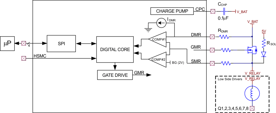 Figure 5-5 GMR, SMR, DMR, and HSMC Register and Application Circuit Diagram
Table 5-6 High-Side Operation Logic
| HSMC PIN | GE_MR BIT | GMR GATE PIN |
|---|---|---|
| LOW | 0 | OFF |
| LOW | 1 | ON |
| HIGH | 0 | ON |
| HIGH | 1 | ON |
| OPEN | 1 | ON |
| OPEN | 0 | OFF |
The overcurrent detection of the external N-MOSFET is triggered by a voltage difference between the DMR and SMR pins in comparator COMP #1. To set the overcurrent threshold, the external series resistor, RDMR, must be sized to generate a particular input voltage (in conjunction with IDMR) on one input of the comparator. The other input voltage of the comparator changes as a function of the RDSON(MAX) and IDS values of the N-MOSFET. By comparing these voltages, the N-MOSFET overcurrent condition is reported. Given the RDSON(MAX) value of the N-MOSFET and the desired overcurrent threshold, RDMR can be calculated using Equation 3.

If the VDS of the N-MOSFET exceeds the threshold set by the comparator for more than the deglitcher time, tOCdet, the GMR pin switches off and the appropriate fault flag (OCMR) is set high. When the overcurrent condition ends, the GMR pin can be switched on again with the SPI enable bit or the external enable pin.
Faults detected on VDD, VBAT, Watchdog (if WD_EN bit is high) prevent the high-side driver from enabling; the GMR pin remains low or turns off. At the time the high-side driver is enabled, the voltage on the GMR pin is tested for a short-to-ground condition only after a certain delay time defined as tSTGPR. If a short is detected the GMR pin remains low. Any time the high-side driver is enabled overcurrent in MOSFET, short-to-ground on the GMR pin, and short-to-ground on the SMR pin can cause a fault condition and disable the high-side driver.
An overvoltage condition (such as a load-dump) on VBAT either turns the GMR pin off or allows it to remain in the previous state depending on the setting of bit 5 (OV_GMR) in register 0x11. With the overvoltage removed, the fault flag FOV can be cleared by reading address 0x00.
The main relay external MOSFET is electrically protected from voltage spikes by an active voltage clamp that limits any voltage levels between GMR and SMR larger than Vgs_clamp.
Load-leakage faults are tested by sourcing a current, ILCdet, out of the SMR pin into the source of the external N-MOSFET. After a time, tLCdet, the SMR voltage is checked to see if it is above VDD. If no leakage is present, the source is above VDD and the GMR pin is turned on. If leakage is present, the source is below VDD and the GMR pin does not turn on. A high on the LMR bit indicates a load-leakage fault. During a load-leakage fault, the SMR pin is biased to the voltage set by the external resistor (RSOL) and a series diode to VDD. Without this path, the SMR pin is floating and may not display faults properly.
Table 5-7 lists a summary of the faults that affect the GMR pin behavior.
Table 5-7 Master Relay Fault and Operation
| SYSTEM EVENT | FAULT BITS AFFECTED | TPIC7218-Q1 STATE | NOTES | |
|---|---|---|---|---|
| BEFORE EVENT |
AFTER EVENT |
|||
| VDD Undervoltage | PORn = 1 | GMR ON | GMR OFF | nRST pin is internally driven low |
| VBAT Overvoltage (>VovVBAT) | FOV = 1 | GMR ON | GMR OFF | OV_GMR = 1 |
| VBAT Overvoltage (>VovVBAT) | FOV = 1 | GMR ON | GMR ON | OV_GMR = 0 |
| VBAT Undervoltage (<VuvVBAT) | FUV = 1 | GMR ON | GMR OFF | |
| Watchdog fault ( must be enabled) | WDSTAT = 0, WD_FAULT = 1 |
GMR ON | GMR OFF | WD_EN = 1 (enabled) |
| nRST pin externally driven low | Erst = 1 | GMR ON | GMR OFF | |
| Overcurrent in master relay | OCMR=1,FHSD = 1 | GMR ON | GMR OFF | OCMRDIS = 0 (disabled) |
| Overcurrent in master relay | OCMR=1,FHSD = 1 | GMR ON | GMR ON | OCMRDIS = 1 (enabled) |
| Short to GND on GMR, while GMR is OFF (time > tSTGMR) | FGMR = 1,FHSD = 1 | GMR OFF | GMR OFF | FGMRDIS = 0 (disabled), turn ON GMR |
| Short to GND on GMR, while GMR is ON | FGMR = 1,FHSD = 1 | GMR ON | GMR OFF | FGMRDIS = 0 (disabled) |
| Short to GND on GMR, while GMR is OFF (time > tSTGMR) | FGMR = 1,FHSD = 1 | GMR OFF | GMR ON | FGMRDIS = 1 (enabled), turn ON GMR |
| Short to GND on GMR, while GMR is ON | FGMR = 1,FHSD = 1 | GMR ON | GMR ON | FGMRDIS = 1 (enabled) |
| Short to GND on SMR | STGMR = 1,FHSD = 1 | GMR ON | GMR OFF | STGMRDIS = 0 (disabled) |
| Short to GND on SMR | STGMR = 1,FHSD = 1 | GMR ON | GMR ON | STGMRDIS = 1 (enabled) |
| GMR is turned on while Q1-Q8 on | LGMR = 1,FHSD = 1 | GMR OFF | GMR OFF | LGMRDIS = 0 (disabled), turn ON GMR |
| GMR is turned on while Q1-Q8 on | LGMR = 1,FHSD = 1 | GMR OFF | GMR ON | LGMRDIS = 1 (enabled), turn ON GMR |
The high-side GMR, SMR, and DMR functionality also includes logic that facilitates system diagnostic testing. The operational status, as well as some fault conditions can be determined for both high-side drivers (HSD) and low-side drivers (LSD). Table 5-8 lists the details.
Table 5-8 High-Side Driver Logic (GMR Only)
| HSD FET | LSD FETx | COMP #1 (HSDC1) |
COMP #2 (HSDC2) |
RESULT |
|---|---|---|---|---|
| ON | OFF | L | L | Normal operating condition for HSD FET |
| ON | OFF | H | L | HSD FET open |
| ON | ON | L | L | Normal operating condition for HSD and LSD FETs |
| ON | ON | H | L | HSD (GMR) FET in overcurrent condition |
| ON | ON | H | H | HSD (GMR) FET in short to ground condition |
| OFF | ON | H | H | Normal operating condition for LSD |
| OFF | ON | H | L | Open load or open LSD FETx |
| OFF | OFF | H | L | Normal operating condition for HSD FET |
| OFF | OFF | H | H | Load short to ground/LSD FETx short to ground |
5.3.9 Wheel-Speed Sensing
The TPIC7218-Q1 device is capable of interfacing with industry standard Active and Intelligent wheel-speed sensors. The TPIC7218-Q1 device features an analog front end that provides power, ground, and interprets current-encoded speed and diagnostic information (Intelligent VDA sensors only) for sensors. Current thresholds can be adjusted to easily interface with most sensors. By setting a voltage on the VREF pin in conjunction with an appropriate current sense resistor, RLOAD, current levels through the wheel-speed sensors are evaluated according to the threshold states. Active wheel-speed sensor current pulse levels can be: undercurrent, overcurrent, wheel-speed-pulse-low (for example 7 mA), and wheel-speed-pulse-high (for example 14 mA). Intelligent wheel-speed sensor current pulse levels can be: undercurrent, overcurrent, wheel-speed-pulse-low (for example 7 mA), wheel-speed-pulse-high (for example 28 mA), and diagnostic-data-bit (for example 14 mA). Wheel-speed-pulse-low and wheel-speed-pulse-high logic state is directly interpreted to a digital voltage output for each sensor (rotational speed). Diagnostic information, diagnostic-data-bit, is directly decoded and placed in four 9-bit registers. Rotational speed information (for two sensors) is also available on high-voltage open-drain outputs. Rotational wheel-speed pulse information for any of the sensors can be MUX-ed into a digital pulse counter. This counter increments on both rising and falling edges. The 8-bit counter, along with other wheel-speed bits are available over SPI. Wheel-speed pins are also electrically protected from typical fault conditions. See Figure 5-6 for register and applications information.
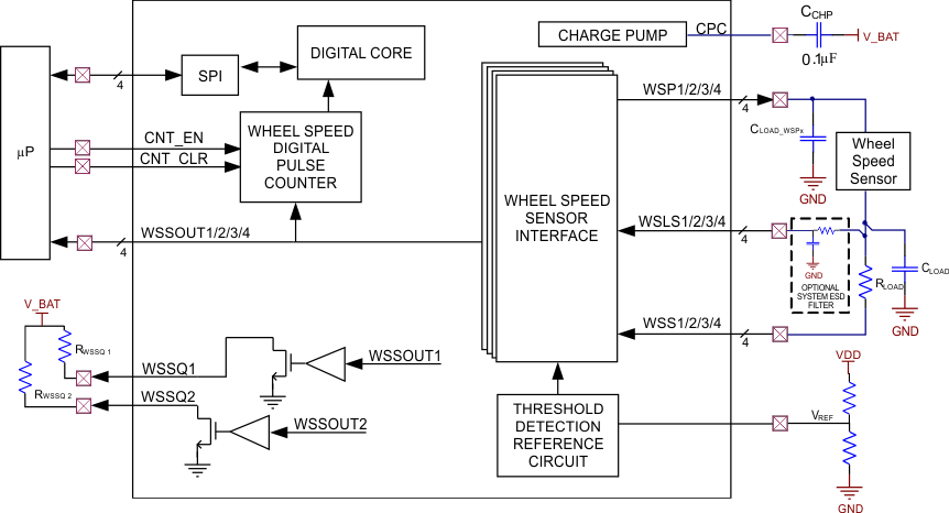 Figure 5-6 Wheel-Speed Register and Application Circuit Diagram
The TPIC7218-Q1 device has three pins for each of the four wheel-speed sensors. The WSPx pins provide a path for current from VBAT to the wheel-speed sensor. The WSLSx pins provide a path for current from the wheel-speed sensor to GND. The WSSx pins monitor current through the sensor by measuring a voltage across the RLOAD resistance, shown in Figure 5-6.
Current is provided to the sensor from the WSP1, WSP2, WSP3, and WSP4 pins. When enabled (by setting the WSPx bits in register 0x1B), the WSPx pins output current and are voltage clamped to Vclamp_WSPx. WSPx pins are electrically protected from short-to-battery, short-to-ground, and overcurrent. Short-to-battery fault bits, WSPx_STB, are located in registers 0x08, 0x0A, 0x0C, 0x0E and overcurrent fault bits, WSPxILIMIT, are located in register 0x1D. If a fault is detected, then the WSPx pins disable. Reading these registers clears the fault bits after the fault condition has been removed.
Current from the sensors is returned to the WSP1, WSP2, WSP3, and WSP4 pins of the TPIC7218-Q1 device, thus providing a path to ground. Current out of the sensor passes through a series resistor, RLOAD, into internal open-drain MOSFETs. These open-drain MOSFETs are controlled by setting the WSLSx bits in register 0x1C. The WSLSx pins are electrically protected from overcurrent by detecting an excessive voltage between WSLSx and WSSx pins. Overcurrent fault bits, WSSxOC, are located in register 0x0F. If a fault is detected then the WSLSx pins stop sinking current. Reading these registers clears the fault bits after the fault is removed.
The sensed voltage difference between the WSSx and WSLSx pins provides the current encoded sensor information to the wheel-speed logic. The WSSx pins are electrically protected from short-to-battery and short-to-ground. These conditions are reported by reading the WSSxOC and WSSxFAULT bits in register 0x0F.
If a fault occurs on WSLSx, the path of the sensor to ground is removed. This type of fault must be cleared by following a specific procedure to prevent an overcurrent fault from being erroneously reported. To clear this fault, first disable the WSPx pins, re-enable the WSLSx pins, and finally re-enable the WSPx pins. The main purpose for this procedure is to first provide a ground path for the sensor before providing power. Other types of faults can be cleared in the normal way, as long as the WSLSx pins are enabled. Table 5-9 lists more information about wheel-speed faults.
Table 5-9 Wheel-Speed Sense Fault and Operation
| SYSTEM EVENT | FAULT BITS AFFECTED | TPIC7218-Q1 | NOTES | |
|---|---|---|---|---|
| PRIOR TO EVENT | POST EVENT | |||
| VDD Undervoltage | PORn = 1 | WSPx ON WSLSx ON WSSQx ON |
WSPx OFF WSLSx OFF WSSQx OFF |
All of the enable bits for these functions are cleared. nRST is driven low. |
| VBAT Overvoltage (>VovVBAT) | FOV = 1 | WSPx ON WSLSx ON WSSQx ON |
WSPx OFF WSLSx OFF WSSQx OFF |
All of the enable bits for these functions are cleared |
| nRST pin externally driven low | Erst = 1 | WSPx ON WSLSx ON WSSQx ON |
WSPx OFF WSLSx OFF WSSQx OFF |
All of the enable bits for these functions are cleared |
| Overcurrent in WSPx | WSPxILIMIT = 1 | WSPx ON WSLSx ON WSSQx ON |
WSPx OFF WSLSx ON WSSQx ON |
WSSQx and WSLSx remain on but no wheel-speed output is produced because the sensor has no power. The enable bits for WSPx remain 1 |
| Overcurrent in WSSx-WSLSx | WSSxOC = 1 | WSPx ON WSLSx ON WSSQx ON |
WSPx ON WSLSx OFF WSSQx ON |
WSPx and WSSQx remain on but no wheel-speed output is produced because the sensor has no ground. The enable bits for WSLSx remain 1 |
| Overcurrent in WSSQx | WSSQxILIMIT = 1 | WSPx ON WSLSx ON WSSQx ON |
WSPx ON WSLSx ON WSSQx OFF |
WSLSx and WSPx remain on. The enable bits for WSSQx remain 1 |
| Short to VBAT on WSPx | WSPx_VBAT = 1 | WSPx OFF WSLSx ON WSSQx ON |
WSPx OFF WSLSx ON WSSQx ON |
This fault is detected only while WSPx are OFF. WSLSx and WSSQx remain unaffected while WSPx is on and shorted to VBAT. |
| Short to GND on WSLSx | WSSxFAULT = 1 | WSPx ON WSLSx ON WSSQx ON |
WSPx ON WSLSx ON WSSQx ON |
WSSQx and WSPx remain on; wheel-speed outputs may be produced but the wheel-speed ground path is not through TPIC7218-Q1 anymore |
| Short to GND on WSSQx | WSSQxFAULT = 1 | WSPx ON WSLSx ON WSSQx OFF |
WSPx ON WSLSx ON WSSQx OFF |
This fault is detected only while WSSQx are off. WSPx and WSLSx remain on and wheel-speed outputs can still be observed. |
The wheel-speed internal equivalent model, shown in Figure 5-7 and Figure 5-8, describe how this functional block works. Users need only select a wheel-speed sensor, current sense resistor, RLOAD, and VREF voltage for basic operation. The wheel-speed functionality is designed to accommodate both Active and Intelligent sensors; the WSSTYPE bit in register 0x1D must be set appropriately.
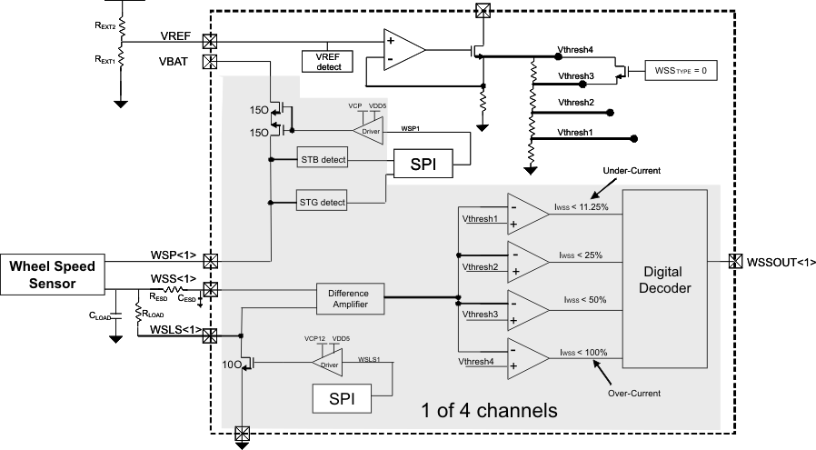 Figure 5-7 Internal Diagram Using Intelligent Type Sensor (WssTYPE = 0)
Table 5-10 Intelligent Sensor Wheel-Speed Thresholds
| THRESHOLD | SIGNIFICANCE | PERCENTAGE OF MAXIMUM THRESHOLD(1) |
|---|---|---|
|
VTHRESH4 |
ISENSOR > ITHRESH4
Overcurrent (possible short to battery) |
100% (40 mA) |
|
VTHRESH3 |
ITHRESH4 > ISENSOR > ITHRESH3
Rotational Wheel-Speed Logic- High |
50% (20 mA) |
|
VTHRESH2 |
ITHRESH3 > ISENSOR > ITHRESH2
Diagnostic sensor Information (9-bit) |
25% (10 mA) |
|
VTHRESH1 |
ISENSOR < ITHRESH1
Undercurrent (possible short to ground) |
11.25% (4.5 mA) |
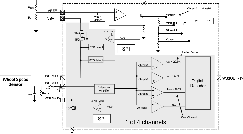 Figure 5-8 Internal Diagram Using Active Type Sensor (WssTYPE = 1)
Table 5-11 Active Sensor Wheel-Speed Thresholds
| THRESHOLD | SIGNIFICANCE | PERCENTAGE OF MAXIMUM THRESHOLD(1) |
|---|---|---|
|
VTHRESH4 |
ISENSOR > ITHRESH4
*Not used |
100% (20 mA) *Not used |
|
VTHRESH3 |
ISENSOR > ITHRESH3
Overcurrent (possible short to battery) |
100% (20 mA) |
|
VTHRESH2 |
ITHRESH3 > ISENSOR > ITHRESH2
Rotational wheel-speed logic- high |
50% (10 mA) |
|
VTHRESH1 |
ISENSOR < ITHRESH1
Undercurrent (possible short to ground) |
22.5% (4.5 mA) |
Both types of sensors provide information based on varying current levels. The TPIC7218-Q1 device provides a way to select different current thresholds by adjusting a voltage on the VREF pin. Internally, the voltage on VREF governs all four thresholds in a ratio metric manner. VREF voltage actually sets the maximum threshold (100%), then, all the other thresholds are automatically set. Intelligent sensors require ITHRESH4 to be set to the maximum threshold, IWSS(overcurrent), and Active sensors require ITHRESH3 to be set to the maximum threshold. For both Intelligent sensors (requiring four thresholds) and Active sensors (requiring three thresholds) use Equation 4 to select a value for VREF.

For example, a typical Intelligent wheel-speed sensor may have a maximum typical current less than 40 mA. This 40-mA current must be set to correspond to VTHRESH4 (100%). If the value of RLOAD is selected as 50 Ω, then the resulting VREF voltage is calculated to be 2 V. Similarly, a typical Active wheel-speed sensor may have a maximum typical current less than 20 mA. This 20-mA current must be set to correspond to VTHRESH3 (100%). However, by setting the WSSTYPE bit, the digital decoder uses VTHRESH3 threshold to actually determine if an overcurrent condition is occurring. By effectively removing the VTHRESH4 resistor in the comparator resistor chain, shown in Figure 5-9, a VREF voltage of 2.4 V and an RLOAD of 120 Ω, are needed to properly set the current thresholds. The ratio of the resistor chain did not change, however the current threshold detection levels did. See Figure 5-9 for more detail.
 Figure 5-9 Example Wheel-Speed Current Pulse Diagram
While selecting RLOAD and VREF, care must be taken so that all electrical specification values are not violated. When the maximum current threshold is selected, the other three thresholds are automatically set.
During normal operation, the WSSOUTx pins provide a digital signal that is high whenever sensor current creates a voltage drop across RLoad that is above the VTHRESH3 level for intelligent sensors and VTHRESH2 level for Active sensors. If the current is less than these respective thresholds, the WSSOUTx pins return to ground. The WSSQ1 and WSSQ2 pins are open-drain outputs that reproduce signals on the WSSOUT1 and WSSOUT2 pins after a propagation delay time of twss_delay. A high level on WSSOUT1 or WSSOUT2 results in low level on WSSQ1 or WSSQ2 pin. These two pins are useful for providing wheel-speed information in a high voltage signal form. The WSSQ1 and WSSQ2 pins also have short-to-ground and open-load detection functionality. The WSSQxFAULT and WSSQxILIMIT bits in register 0x05 report these faults and are cleared by reading them after the removal of the fault condition. During an overcurrent fault the WSSQ1 and WSSQ2 pins remain enabled for a time of tdelay_WSSQx. After this time these pins are disabled.
The TPIC7218-Q1 device also features an 8-bit wheel-speed pulse counter. This counter increments on every rising and falling edge of a selected WSSOUTx. A MUX selects which the WSSOUTx signal is input to the counter; bits WS_Cnt_MUX[1] and WS_Cnt_MUX[0] program the MUX as listed in Table 5-12. Count data is reported in register 0x04. A high on the CNT_EN pin allows the counter to increment. A high on the CNT_CLR pin forces the counter to reset to 0. The count value is available for read through SPI at any point. If the counter is allowed to reach maximum value, the count value remains at maximum but an overflow bit, WSS_OV_Cnt is set. If both CNT_CLR and CNT_EN pins are in a high logic state then the WS_Fail_Cnt bit is set. These bits clear on read after the fault conditions have been removed.
Table 5-12 Wheel-Speed Counter Input
| WS_Cnt_MUX[1] | WS_Cnt_MUX[0] | SELECTED INPUT |
|---|---|---|
| 0 | 0 | WSSOUT1 |
| 1 | 0 | WSSOUT2 |
| 0 | 1 | WSSOUT3 |
| 1 | 1 | WSSOUT4 |
When the TPIC7218-Q1 device is paired with VDA protocol compatible Intelligent wheel-speed sensors, additional functionality for processing and reporting diagnostic information can be enabled. Diagnostic encoded data (Manchester encoded) in the form of current pulses reaching the ITHRESH2 (10 mA) threshold are decoded and placed in the WSSxDx bits. All nine bits are available for reading. If any of the (nine) bit pulse widths were outside the allowed pulse width range (36 μs to 64 μs including variations) then the pulse widths are not counted as valid. As each of the nine bits are input, only valid bits cause the WSSx_Valid counter to increment. In this way information about bit errors, or fewer than nine bits being sent from the sensor is recorded and available for each wheel-speed channel. The TPIC7218-Q1 device also contains logic to determine when a new 9-bit frame has started to be input. When detected, the WSSx_New bit is set. If the wheel-speed sensor is in stand still mode then the TPIC7218-Q1 device detects this current pulse activity, resulting in the WSS_MODE bit being set. Both of these bits can be cleared upon read.
5.3.10 K-Line
The TPIC7218-Q1 device includes a serial communication transceiver for K-Line. K-Line provides a bi-directional half-duplex interface for automotive diagnostic communication with data transfer rates of up to 10.4 kbps. The integrated transceiver conforms to the ISO-9141 standard and meets the on-board diagnostic (OBD) requirements of the California Air Resources Board (CARB). For more information on the K-Line protocol see the compete K-Line standard.
Features of the K-Line module include the following:
- ISO-K operates over a wide signal voltage range and is capable of driving high currents.
- ISO-K pin can tolerate a parasitic capacitance of up to 10 nF.
- ISO-K pin is electrically protected to withstand short-to-ground and overcurrent faults.
- The driver stage of the ISO-K pin is thermally protected. A temperature fault disables the bus. Thermal protection also includes hysteresis and blank time before restarting.
- KRx and KTx directly interface to both 5-V and 3.3-V microprocessors without the need for pullup resistors.
- K-Line continues to function regardless of any TPIC7218-Q1 fault conditions with the exception of VDD undervoltage reset condition which powers down the entire TPIC7218-Q1 device.
 Figure 5-10 K-Line Application Schematic
5.3.11 Warning Lamp Drivers
The TPIC7218-Q1 device features three output pins for warning lamps. The WLQ1 and WLQ2 pins are high voltage low-side drivers. The WL_LS pin is a low voltage low-side driver.
The WL_LS driver enables whenever the watchdog controlled bit, WD_STAT, is high. This low-side driver is an open-drain MOSFET; to realize a high logic level and external pullup resistor must be used. Driver operation is only dependent on a watchdog fault.
The WLQ1 driver enables whenever the WLG1 pin and the GE_9 bit is set. The WLQ2 driver works in the same way utilizing the WLG2 pin and the GE_10 bit. Each driver is monitored for three fault conditions: overcurrent, open-load, and over-temperature. However, driver operation also depends on other fault conditions: VDD undervoltage, and watchdog fault. See the application circuit and register diagram in Figure 5-11.
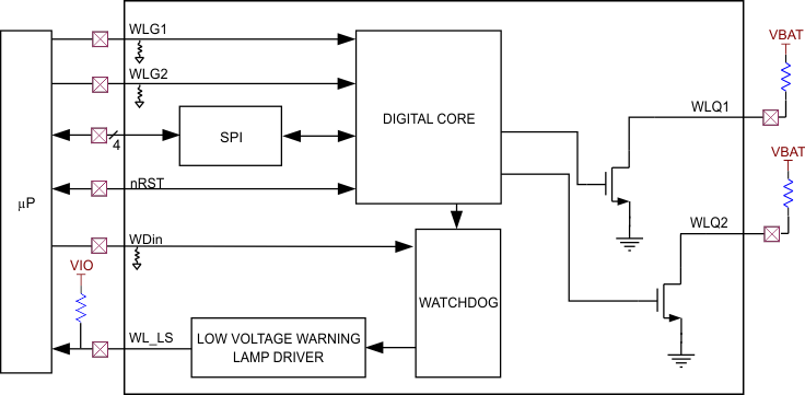 Figure 5-11 Warning Lamp Driver Register and Application Circuit Diagram
Each digital driver monitors, reports, and has integrated protection for many electrical fault conditions. Overcurrents are reported as a 1 in register 0x03, (bits 0 and 2 are referenced by bits F9, F10) and do not cause the affected driver to disable. Overcurrents are merely reported after a deglitch time of toff_blank_WLQx. Over-temperature (junction) faults are reported in register 0x03, (bit-6 OTSD) and cause both drivers to disable after a deglitch time of toff_tmp_WLQx.. The high-voltage warning-lamp drivers are also checked for an open-load or short to ground condition whenever they are not enabled. This type of fault causes register 0x03, (bits 1 and 3 are referenced by bits S9 and S10) to be reported as a 1. A master low-side fault bit in register 0x00, (bit-0) becomes high whenever an overcurrent or open-load fault occurs. Faults can be cleared by reading the appropriate fault reporting register. When this occurs, the low-side master fault bit (FAIL) can be cleared by reading it.
The high-voltage warning-lamp drivers also respond to fault conditions within other functional blocks. These drivers are disabled whenever the VDD undervoltage fault bit in register 0x00 is set. Also, a watchdog fault can cause these drivers to disable, if register 0x11, bit-4 (WD_EN) is set. This bit defaults to 0 upon power up. Any of these faults do not cause the FAIL bit to be set.
Faults can be cleared by reading the appropriate fault reporting register. When this occurs the digital drivers can be re-enabled. Fault reporting bits do not have any affect on these warning lamp drivers; only the actual fault condition causes a driver to disable. Nevertheless, TI recommends clearing the fault bits by reading them before enabling the drivers.
Aside from monitoring and reporting faults, the high-voltage warning-lamp drivers have overvoltage protection circuitry built in. An active-clamp monitors voltage on the pins of these drivers. Voltages larger than Vcl_WLQx are clamped.
5.3.12 Watchdog Operation
The TPIC7218-Q1 device also features watchdog functionality. Watchdog functionality is programmable and can be disabled. This functional block receives clock pulses from an external microprocessor through WDIN pin to verify proper system operation. Whenever a watchdog fault occurs, the low-voltage warning-lamp pin (WL_LS), the reset pin (nRST), and many of the other functional blocks within the TPIC7218-Q1 device are affected. The TPIC7218-Q1 device can be set to accept a range of different pulse widths for easy connection to most microprocessors.
If watchdog functionality is enabled (WD_EN = 1), the TPIC7218-Q1 logic monitors WDIN pulse widths by counting the number of internal clocks that occur between WDIN rising and falling edges. Two, 2-bit values ( WDH<1:0>, WDL<1:0>) can be adjusted to select the length of a valid window range for a WDIN pulse. Pulse widths inside of this window range are counted as a good pulse. A good pulse increments a 3-bit state machine counter by one (WDCNTx bits, in register 0x05). When a counter value of 7 is reached, the status bit, WDSTAT , becomes a 1 and all TPIC7218-Q1 watchdog inhibited functionality is enabled. If a bad pulse occurs then the state machine counter is decremented by three. The WD_FAULT bit is set whenever the counter value is 0, causing the WD_STAT bit to become low. A fault turns off high-side drivers, low-side drivers, wheel-speed functionality, and high-voltage warning-lamp drivers. Both the low-voltage warning-lamp driver (WL_LS) and the reset pin (nRST) enables. The SPI continues to function and the WD_FAULT and WDSTAT bits indicate a watchdog fault. When a full watchdog count is reached, register bits and functionality would return to normal state. Refer to Figure 5-12 through Figure 5-14 for more details on the state transitions and timing.
If the WDIN pin does not realize a transition after twice the length of time selected in the upper window, which is set by bits WDH<1:0>, then an out-of-range condition occurs. The watchdog fault becomes high and the watchdog status bit becomes low (WD_FAULT = 1, and WDSTAT = 0).
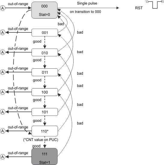 Figure 5-12 Watchdog State Transition Diagram
 Figure 5-13 Timing Diagram Showing A Bad Pulse
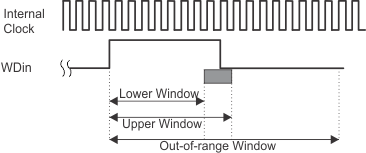 Figure 5-14 Timing Diagram Showing A Good Pulse
5.4 Device Functional Modes
The device operates in normal mode as described in Section 5.3 unless it is in the reset state.
5.4.1 Device Reset
Several events cause the TPIC7218-Q1 device to reset. For a compete view of TPIC7218-Q1 behavior during reset, refer to Table 5-1.
-
Power-On Reset A power-on reset, POR, is caused when the VDD supply voltage falls below the reset threshold. On POR the nRST pin is pulled low by the TPIC7218-Q1 device.
-
Watchdog ResetA watchdog reset is initiated whenever the Watchdog counter decrements to 000. Upon Watchdog Reset, the nRST pin is pulsed low, and the WDSTAT flag is cleared. As the nRST pin is released, the Watchdog state machine is restarted. The watchdog will re-enable after a delay time TWD_PULSE to allow sufficient time for the microcontroller to reset.
-
External ResetAn external reset is realized whenever the nRST pin is driven low by an external signal (usually from a microprocessor). When nRST is released the Erst bit is set, indicating that an external reset occurred.
5.5 Programming
5.5.1 Serial Peripheral Interface (SPI) Interface To Microcontroller
The TPIC7218-Q1 device uses a SPI communication interface. The TPIC7218-Q1 device operates as a slave with full-duplex, synchronous, 8-bit transfer frames. The device can be controlled and monitored in one of three modes: Read, Write, and Dummy. Read command returns data to the master. If a fault register is read, then any faults will be cleared. However, if the fault still exists then the fault reporting bit(s) will remain high. A write command sends data to the slave. Data is latched in on the rising edge of the second chip select. A dummy command is used whenever the master and slave loose synchronization. This happens whenever the master does not issue a normal 16 bit transfer using two eight bit frames. Dummy commands essentially reset the SPI logic to the default state.
A typical SPI operation contains two full chip select frames; each containing eight clock pulses. All SPI transaction starts when CSN transitions to a logic low. During this time 8-bits of mode, R/W, and address data are clocked into SI. Finally, the CSN returns high, concluding the first half of the normal transaction. The second half of the normal transaction starts when CSN again transitions to a logic low. During this time 8-bits of data are clocked into SI. Finally, the CSN returns high, and a normal SPI transaction is concluded. If one chip-select frame does not have exactly eight clocks, then the whole 16-bit transaction is considered invalid and is ignored. The CSN must go high for a window of 2 μs to 28 μs (CSNtimeout) between two 8-bit commands for the 16-bit command to be considered valid. A 16-bit read command consists of an 8-bit read command of the intended address and an 8-bit dummy command. The SPI can also operate in burst mode, whereby consecutive 8-bit read commands result in a consecutive 8-bit data being returned to the master.
Table 5-13 SPI Instruction Encoding
| MODE | R/Wn | STAT. | A[5] | A[4] | A[3] | A[2] | A[1] | A[0] |
|---|---|---|---|---|---|---|---|---|
| Unused | 0 | 1 | A[5] | A[4] | A[3] | A[2] | A[1] | A[0] |
| Read | 1 | 0 | A[5] | A[4] | A[3] | A[2] | A[1] | A[0] |
| Write | 0 | 0 | A[5] | A[4] | A[3] | A[2] | A[1] | A[0] |
| Dummy | 1 | 1 | X | X | X | X | X | X |
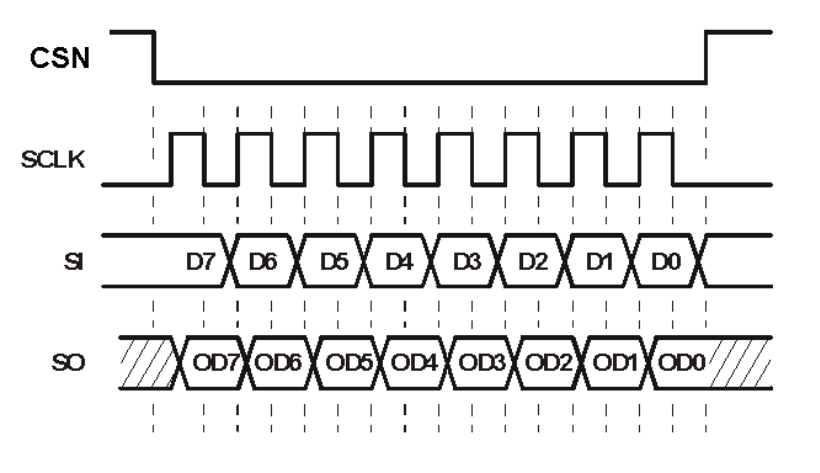 Figure 5-15 One Chip-Select Frame
The SO pin contains the register data in response to the previous eight bit frame. Data out is always delayed by one SPI transfer (for example, response to the command N is shifted out at the same time command N+1 is shifted in). Valid data is shifted out from the SO pin on the rising edge of SCLK. The response to the SPI frame depends on which type of transaction mode is requested by the Master (read, write, or dummy).
If the SPI transaction is valid, the Slave determines what type of operation is being requested. If a Read transaction is requested, the Slave responds with the Read byte during the next SPI transaction. Figure 5-16 shows the SPI Read operation.
 Figure 5-16 One Chip-Select Frame
A Write operation places the data byte into the address specified in the previous chip select frame.
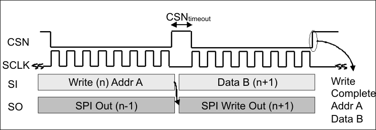 Figure 5-17 One Chip-Select Frame
5.5.1.1 Summary and Description Of Control and Reporting Registers
The TPIC7218-Q1 device contains 30 registers that contain both fault reporting and control bits. Refer to the following tables for register map and functional description of each bit.
5.6 Register Maps
5.6.1 SPI Registers
Table 5-14 SPI Registers Map
| ADDRESS | R/W | b7 | b6 | b5 | b4 | b3 | b2 | b1 | b0 |
|---|---|---|---|---|---|---|---|---|---|
| 0x00 | R | HSDC2 | FHSD | FOV | FUV | Erst | HSDC1 | PORn | FAIL |
| 0x01 | R | S4 | F4 | S3 | F3 | S2 | F2 | S1 | F1 |
| 0x02 | R | S8 | F8 | S7 | F7 | S6 | F6 | S5 | F5 |
| 0x03 | R | WS_OV_Cnt | OTSD | WS_Fail_Cnt | KI | S10 | F10 | S9 | F9 |
| 0x04 | R | WS_Cnt_OUT7 | WS_Cnt_OUT6 | WS_Cnt_OUT5 | WS_Cnt_OUT4 | WS_Cnt_OUT3 | WS_Cnt_OUT2 | WS_Cnt_OUT1 | WS_Cnt_OUT0 |
| 0x05 | R | WSSQ2ILIMIT | WSSQ1ILIMIT | WSSQ2FAULT | WSSQ1FAULT | WDSTAT | WDCNT2 | WDCNT1 | WDCNT0 |
| 0x06 | R | VLDDEG | OCPR | STGPR | FGPR | LMR | FGMR | STGMR | OCMR |
| 0x07 | R | WSS1D7 | WSS1D6 | WSS1D5 | WSS1D4 | WSS1D3 | WSS1D2 | WSS1D1 | WSS1D0 |
| 0x08 | R | WSS1_Valid3 | WSS1_Valid2 | WSS1_Valid1 | WSS1_Valid0 | WSP1_STB | WSS1_Mode | WSS1_New | WSS1D8 |
| 0x09 | R | WSS2D7 | WSS2D6 | WSS2D5 | WSS2D4 | WSS2D3 | WSS2D2 | WSS2D1 | WSS2D0 |
| 0x0A | R | WSS2_Valid3 | WSS2_Valid2 | WSS2_Valid1 | WSS2_Valid0 | WSP2_STB | WSS2_Mode | WSS2_New | WSS2D8 |
| 0x0B | R | WSS3D7 | WSS3D6 | WSS3D5 | WSS3D4 | WSS3D3 | WSS3D2 | WSS3D1 | WSS3D0 |
| 0x0C | R | WSS3_Valid3 | WSS3_Valid2 | WSS3_Valid1 | WSS3_Valid0 | WSP3_STB | WSS3_Mode | WSS3_New | WSS3D8 |
| 0x0D | R | WSS4D7 | WSS4D6 | WSS4D5 | WSS4D4 | WSS4D3 | WSS4D2 | WSS4D1 | WSS4D0 |
| 0x0E | R | WSS4_Valid3 | WSS4_Valid2 | WSS4_Valid1 | WSS4_Valid0 | WSP4_STB | WSS4_Mode | WSS4_New | WSS4D8 |
| 0x0F | R | WSS4OC | WSS3OC | WSS2OC | WSS1OC | WSS4FAULT | WSS3FAULT | WSS2FAULT | WSS1FAULT |
| 0x10 | RW | GE8 | GE7 | GE6 | GE5 | GE4 | GE3 | GE2 | GE1 |
| 0x11 | RW | WD_Fault | 0 | OV_GMR | WD_EN | GE_PR | GE_MR | GE10 | GE9 |
| 0x12 | RW | WDH<1> | WDH<0> | WDL<1> | WDL<0> | PWMFreq1 | PWMFreq0 | WS_Cnt _MUX[1] | WS_Cnt _MUX[0] |
| 0x13 | RW | PWMQ5<7> | PWMQ5<6> | PWMQ5<5> | PWMQ5<4> | PWMQ5<3> | PWMQ5<2> | PWMQ5<1> | PWMQ5<0> |
| 0x14 | RW | 0 | 0 | 0 | 0 | PWMQ5Phase<1> | PWMQ5Phase<0> | PWMQ5<9> | PWMQ5<8> |
| 0x15 | RW | PWMQ6<7> | PWMQ6<6> | PWMQ6<5> | PWMQ6<4> | PWMQ6<3> | PWMQ6<2> | PWMQ6<1> | PWMQ6<0> |
| 0x16 | RW | 0 | 0 | 0 | 0 | PWMQ6Phase<1> | PWMQ6Phase<0> | PWMQ6<9> | PWMQ6<8> |
| 0x17 | RW | PWMQ7<7> | PWMQ7<6> | PWMQ7<5> | PWMQ7<4> | PWMQ7<3> | PWMQ7<2> | PWMQ7<1> | PWMQ7<0> |
| 0x18 | RW | 0 | 0 | 0 | 0 | PWMQ7Phase<1> | PWMQ7Phase<0> | PWMQ7<9> | PWMQ7<8> |
| 0x19 | RW | PWMQ8<7> | PWMQ8<6> | PWMQ8<5> | PWM4Q8<4> | PWMQ8<3> | PWMQ8<2> | PWMQ8<1> | PWMQ8<0> |
| 0x1A | RW | 0 | 0 | 0 | 0 | PWMQ8Phase<1> | PWMQ8Phase<0> | PWMQ8<9> | PWMQ8<8> |
| 0x1B | RW | 0 | WSSP4 | WSSP3 | WSSP2 | WSSP1 | WSSTYPE | WSSQ2 | WSSQ1 |
| 0x1C | RW | OCPRDIS | STGPRDIS | OCMRDIS | STGMRDIS | WSLS4 | WSLS3 | WSLS2 | WSLS1 |
| 0x1D | RW/R* | VREFOK* | FGPRDIS | FGMRDIS | LMRDIS | WSP4ILIMIT | WSP3ILIMIT* | WSP2ILIMIT* | WSP1ILIMIT* |
Table 5-15 Description Of Control and Reporting Bits
| BIT NAME | DESCRIPTION |
|---|---|
| Fail |
Any fault on any digital or PWM low-side driver 0 = Fault not detected 1 = Fault detected |
| PORn |
Power-on reset. Reset low when read by microcontroller. 0 = No power-on reset detected. Reset to this value when read by microcontroller. 1 = Power-on reset detected |
| HSDC1 |
High-side driver comparator1 for Master Relay (MR) 0 = Comparator output low 1 = Comparator output high |
| Erst |
RST pin is pulled low by external source 0 = Fault not detected 1 = Fault detected |
| Fuv |
Undervoltage on VBAT 0 = Fault not detected 1 = Fault detected |
| Fov |
Overvoltage on VBAT 0 = Fault not detected 1 = Fault detected |
| FHSD |
Any fault on the high-side drivers (either GMR or GPR). If set, this bit is latched until Address 6 is read. Then, it clears on read. 0 = Fault not detected 1 = Fault detected |
| HSDC2 |
High-side driver comparator 2 for Master Relay (MR) 0 = Comparator output low 1 = Comparator output high |
| Sx |
Open-load fault on the low-side output (S9 reports WLQ1 fault and S10 reports WLQ2 fault) 0 = Fault not detected on output x 1 = Fault detected on output x |
| Fx |
Short-to-battery fault on the low-side output (F9 reports WLQ1 fault and F10 reports WLQ2 fault) 0 = Fault not detected on output x 1 = Fault detected on output x |
| WS_Fail_Cnt |
CNT_EN and CNT_CLR set at the same time 0 = Fault not detected 1 = Fault detected |
| Kl |
Status bit for Kline current limit condition 0 = Fault not detected 1 = Fault detected |
| OTSD |
Any overtemperature fault 0 = Fault not detected 1 = Fault detected |
| WS_OV_Cnt |
Count overflow on the wheel-speed sensor (past 256) 0 = Overflow not detected 1 = Overflow detected |
| WSSx_Valid4 | This word shows the valid number of bits in each wheel-speed channel. |
| WSSx_Valid3 | |
| WSSx_Valid2 | |
| WSSx_Valid1 | |
| WDCNT0 | Status Bit 1 of three that is used to track the operation of the watchdog circuit (LSB) |
| WDCNT1 | Status Bit 2 of three that is used to track the operation of the watchdog circuit |
| WDCNT2 | Status Bit 3 of three that is used to track the operation of the watchdog circuit (MSB) |
| WDSTAT |
Watchdog status bit 0 = Out-of-range 1 = In-range |
| WSSQ1FAULT |
Open load or short to ground on WSSQ1 0 = Fault not detected 1 = Fault detected |
| WSSQ2FAULT |
Open load or short to ground on WSSQ2 0 = Fault not detected 1 = Fault detected |
| WSSQ1ILIMIT |
Overcurrent on WSSQ1 0 = Fault not detected 1 = Fault detected |
| WSSQ2ILIMIT |
Overcurrent on WSSQ2 0 = Fault not detected 1 = Fault detected |
| OCMR |
Overcurrent fault on MR 0 = Fault not detected 1 = Fault detected |
| STGMR |
Short-to-ground fault on MR 0 = Fault not detected 1 = Fault detected |
| FGMR |
GMR disabled by external circuitry 0 = GMR not disabled 1 = GMR disabled |
| LMR |
Load-leakage fault on MR (Master Relay) 0 = Fault not detected 1 = Fault detected |
| FGPR |
GPR disabled by external circuitry 0 = GPR not disabled 1 = GPR disabled |
| STGPR |
Short-to-ground fault on PR 0 = Fault not detected 1 = Fault detected |
| OCPR |
Overcurrent fault on PR 0 = Fault not detected 1 = Fault detected |
| VLD DEG | This bit is a replica of FOV |
| WSS1Dx | VDA data bits for wheel-speed channel 1 |
| WSS2Dx | VDA data bits for wheel-speed channel 2 |
| WSS3Dx | VDA data bits for wheel-speed channel 3 |
| WSS4Dx | VDA data bits for wheel-speed channel 4 |
| WSSx_New |
Flag bits that notify the availability of new data for each sensor channel 1 = new data since last read was performed 0 = old data since last read was performed |
| WSSx_Mode |
Flag bits that notify the mode of operation for each sensor channel 1 = standstill mode 0 = normal mode |
| WSPx_STB |
Flag bits that show a short to battery for each sensor channel in the off state 1 = short to battery 0 = normal operation |
| WS_Cnt_OUT7 | Bit 7 of wheel-speed counter (value latched at CSN low-to-high transition) |
| WS_Cnt_OUT6 | Bit 6 of wheel-speed counter |
| WS_Cnt_OUT5 | Bit 5 of wheel-speed counter |
| WS_Cnt_OUT4 | Bit 4 of wheel-speed counter |
| WS_Cnt_OUT3 | Bit 3 of wheel-speed counter |
| WS_Cnt_OUT2 | Bit 2 of wheel-speed counter |
| WS_Cnt_OUT1 | Bit 1 of wheel-speed counter |
| WS_Cnt_OUT0 | Bit 0 of wheel-speed counter |
| WSSxFAULT |
Open load or short to ground on WSSx pins 0 = Fault not detected 1 = Fault detected |
| WSSxOC |
Overcurrent fault on WSSx pins 0 = Fault not detected 1 = Fault detected |
| GE1 | Enable and disable digital driver 1. It does not clear on Q1 fault |
| GE2 | Enable and disable digital driver 2. It does not clear on Q2 fault |
| GE3 | Enable and disable digital driver 3. It does not clear on Q3 fault |
| GE4 | Enable and disable digital driver 4. It does not clear on Q4 fault |
| GE5 | Enable and disable digital driver 5. It does not clear on Q5 fault |
| GE6 | Enable and disable digital driver 6. It does not clear on Q6 fault |
| GE7 | Enable and disable digital driver 7. It does not clear on Q7 fault |
| GE8 | Enable and disable digital driver 8. It does not clear on Q8 fault |
| GE9 | Enable and disable warning lamp driver 1. It does not clear on WLQ1 fault |
| GE10 | Enable and disable warning lamp driver 2. It does not clear on WLQ2 fault |
| GE_MR | Enable and disable Master Relay (GMR). It clears on fault |
| GE_PR | Enable and disable pump motor relay (GPR). It clears on fault |
| WD_EN |
Watchdog state machine enable. 1 = Enabled; Q1-Q8, GMR, GPR cannot be turned on unless WDSTAT =1 0 = Disabled; Q1-Q8, GMR, GPR can be controlled independent of WDstat. (WDSTAT =0 when WD_EN=0) |
| OV_GMR |
Configure the response of GMR FET during overvoltage condition 0 = Maintain the previous state 1 = Disable GMR FET |
| WD_FAULT |
Status bit that latches the watchdog fault WDSTAT=0. It clears on read and it is a read only bit 1 = watchdog fault has happened (WDSTAT =0) 0 = no watchdog fault has happened (WDSTAT =1) |
| WS_Cnt_MUX1 | Control bit 1 for wheel-speed sensor multiplexer |
| WS_Cnt_MUX0 | Control bit 0 for wheel-speed sensor multiplexer |
| PWMFreq<1:0> | Control bits to set the PWM frequency |
| WDH<1:0> |
Control bits to set the watchdog upper window range 00 = 64 ms 01 = 32 ms 10 = 16 ms 11 = 8 ms |
| WDL<1:0> |
Control bits to set the watchdog lower window range 00 = 32 ms 01 = 16 ms 10 = 8 ms 11 = 4 ms |
| PWMQx<9:0> | Control bits to set the duty cycle of each PWM channel. When changing from one duty cycle setting to another, the new setting takes place in the next period. |
| PWMQxPhase<1:0> |
Control bits to set the phase shift for the PWM drivers 00=0° 01=90° 10=180° 11=270° |
| WSSQ1 | Enable and disable wheel-speed output WSSQ1. It clears only on VBAT overvoltage fault |
| WSSQ2 | Enable and disable wheel-speed output WSSQ1. It clears only on VBAT overvoltage fault |
| WSSTYPE |
Type of sensor used 1 = Active 0 = Intelligent |
| WSPx |
Control bit for the supply of the wheel-speed sensor. It clears only on VBAT overvoltage fault 1 = ON 0 = OFF |
| WSLSx |
Control bit for the supply return of the wheel-speed sensor. It clears only on VBAT overvoltage fault 1 = ON 0 = OFF |
| STGMRDIS |
Enable and disable MR short-to-ground protection (STGMR) 0 = Disabled (default after reset) 1 = Enabled |
| OCMRDIS |
Enable and disable MR overcurrent protection (OCMR) 0 = Disabled (default after reset) 1 = Enabled |
| STGPRDIS |
Enable and disable PR short-to-ground protection (STGPR) 0 = Disabled (default after reset) 1 = Enabled |
| OCPRDIS |
Enable and disable PR overcurrent protection (OCPR) 0 = Disabled (default after reset) 1 = Enabled |
| WSPxILIMIT |
Current limit fault on WSPx pins (read only bits) 0 = Fault not detected 1 = Fault detected |
| LMRDIS |
Enable and disable MR leakage protection (LMR) 0 = Disabled (default after reset) 1 = Enabled |
| VREFOK |
Status bit that indicates if VREF pin is more than 0.75 V (read only) 0 = VREF pin is less than 0.75 V 1 = VREF pin is more than 0.75 V |