SLVS817G May 2008 – June 2015 TPD4S009 , TPD4S010
PRODUCTION DATA.
- 1 Features
- 2 Applications
- 3 Description
- 4 Revision History
- 5 Pin Configuration and Functions
- 6 Specifications
-
7 Detailed Description
- 7.1 Overview
- 7.2 Functional Block Diagram
- 7.3
Feature Description
- 7.3.1 ±8-kV IEC61000-4-2 Level 4 Contact ESD Protection
- 7.3.2 IEC61000-4-5 Surge Protection
- 7.3.3 I/O Capacitance
- 7.3.4 Low Leakage Current
- 7.3.5 Supports High-Speed Differential Data Rates
- 7.3.6 Ultra-low Matching Capacitance Between Differential Signal Pairs
- 7.3.7 Ioff Feature for the TPD4S009
- 7.3.8 Industrial Temperature Range
- 7.3.9 Easy Flow-Through Routing
- 7.4 Device Functional Modes
- 8 Application and Implementation
- 9 Power Supply Recommendations
- 10Layout
- 11Device and Documentation Support
- 12Mechanical, Packaging, and Orderable Information
封装选项
机械数据 (封装 | 引脚)
散热焊盘机械数据 (封装 | 引脚)
- DRY|6
订购信息
6 Specifications
6.1 Absolute Maximum Ratings
over operating free-air temperature range (unless otherwise noted)| MIN | MAX | UNIT | |||
|---|---|---|---|---|---|
| VCC | Supply voltage range for TPD4S009 | –0.3 | 6 | V | |
| VIO | IO signal voltage range | 0 | VCC | V | |
| TA | Characterized free-air operating temperature range | –40 | 85 | °C | |
| Lead temperature, 1.6 mm (1/16 in) from case for 10 s) | 260 | °C | |||
| Peak pulse power (tp = 8/20 μs) | 25 | W | |||
| Peak pulse current (tp = 8/20 μs) | 2.5 | A | |||
| Tstg | Storage temperature range | –65 | 125 | °C | |
6.2 ESD Ratings
| VALUE | UNIT | |||
|---|---|---|---|---|
| V(ESD) | Electrostatic discharge | Human body model (HBM), per ANSI/ESDA/JEDEC JS-001(1) | ±2500 | V |
| Charged-device model (CDM), per JEDEC specification JESD22-C101(2) | ±1500 | |||
| IEC 61000-4-2 Contact Discharge | ±8000 | |||
| IEC 61000-4-2 Air-Gap Discharge | ±9000 | |||
(1) JEDEC document JEP155 states that 500-V HBM allows safe manufacturing with a standard ESD control process.
(2) JEDEC document JEP157 states that 250-V CDM allows safe manufacturing with a standard ESD control process.
6.3 Recommended Operating Conditions
over operating free-air temperature range (unless otherwise noted)| MIN | NOM | MAX | UNIT | ||
|---|---|---|---|---|---|
| TA Operating free-air Temperature Range | -40 | 85 | °C | ||
| Operating Voltage | VCC Pin | 0.9 | 5.5 | V | |
| IOx Pin (TPD4S009) | 0 | VCC | |||
| IOx Pin (TPD4S010) | 0 | 5.5 | |||
6.4 Thermal Information
| THERMAL METRIC(1) | TPD4S009 | TPD4S010 | UNIT | ||||
|---|---|---|---|---|---|---|---|
| DBV (SOT) | DCK (SOT) | DGS (VSSOP) | DRY (USON) | DQA (USON) | |||
| 6 PINS | 6 PINS | 10 PINS | 6 PINS | 10 PINS | |||
| RθJA | Junction-to-ambient thermal resistance | 201.7 | 254.4 | 205.0 | 380.55 | 265.3 | °C/W |
| RθJC(top) | Junction-to-case (top) thermal resistance | 175.0 | 123.9 | 76.1 | 229.07 | 129.4 | °C/W |
| RθJB | Junction-to-board thermal resistance | 47.6 | 94.0 | 126.0 | 235.57 | 189.7 | °C/W |
| ψJT | Junction-to-top characterization parameter | 52.8 | 14.5 | 9.4 | 56.76 | 31.1 | °C/W |
| ψJB | Junction-to-board characterization parameter | 47.1 | 92.3 | 124.3 | 232.80 | 189.7 | °C/W |
| RθJC(bot) | Junction-to-case (bottom) thermal resistance | N/A | N/A | N/A | 91.03 | N/A | °C/W |
(1) For more information about traditional and new thermal metrics, see the Semiconductor and IC Package Thermal Metrics application report, SPRA953.
6.5 Electrical Characteristics
over operating free-air temperature range (unless otherwise noted)| PARAMETER | TEST CONDITIONS | MIN | TYP | MAX | UNIT | ||||
|---|---|---|---|---|---|---|---|---|---|
| VRWM | Reverse standoff voltage | Any IO pin to ground | 5.5 | V | |||||
| VBR | Breakdown voltage | IIO = 1 mA | Any IO pin to ground | 9 | V | ||||
| IIO | IO port current | VIO = 3.3 V, VCC = 5 V | Any IO pin | 0.01 | 0.1 | μA | |||
| Ioff | Current from IO port to supply pins | VIO = 3.3 V, VCC = 5 V | Any IO pin | 0.01 | 0.1 | μA | |||
| VD | Diode forward voltage | IIO = 8 mA | Lower clamp diode | 0.6 | 0.8 | 0.95 | V | ||
| RDYN | Dynamic resistance | I = 1 A | Any IO pin | 1.1 | Ω | ||||
| CIO | IO capacitance | VCC = 5 V, VIO = 2.5 V | Any IO pin | 0.8 | pF | ||||
| ICC | Operating supply current | VIO = Open, VCC = 5 V | VCC pin | 0.1 | 1 | μA | |||
6.6 Typical Characteristics
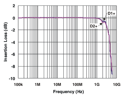 Figure 1. Insertion Loss S21 – I/O to GND
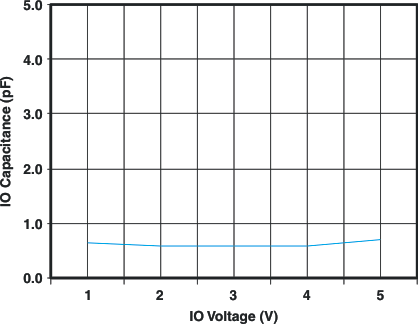
VCC = 5 V
Figure 3. IO Capacitance vs Input Voltage
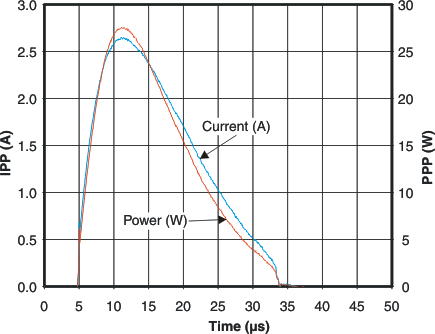
8/20 μs Pulse
Figure 5. Pulse Waveform
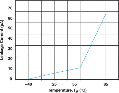
VIO = 2.5 V
Figure 2. Leakage Current vs Temperature
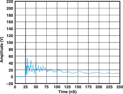
8-kV Contact, Average of Ten Waveforms
Figure 4. IEC Clamping Waveforms