ZHCSCO4C May   2014  – February 2017 TPD4E6B06

PRODUCTION DATA.  

  1. 特性
  2. 应用
  3. 说明
  4. 修订历史记录
  5. Pin Configuration and Functions
  6. Specifications
    1. 6.1 Absolute Maximum Ratings
    2. 6.2 ESD Ratings
    3. 6.3 Recommended Operating Conditions
    4. 6.4 Thermal Information
    5. 6.5 Electrical Characteristics
    6. 6.6 Typical Characteristics
  7. Detailed Description
    1. 7.1 Overview
    2. 7.2 Functional Block Diagram
    3. 7.3 Feature Description
      1. 7.3.1 IEC 61000-4-2 Level 2 ESD Protection
      2. 7.3.2 IEC 61000-4-5 Surge Protection
      3. 7.3.3 IO Capacitance
      4. 7.3.4 RDYN
      5. 7.3.5 DC Breakdown Voltage
      6. 7.3.6 Ultra-Low Leakage Current
      7. 7.3.7 Clamping Voltage
      8. 7.3.8 Industrial Temperature Range
      9. 7.3.9 Space Saving DPW Package
    4. 7.4 Device Functional Modes
  8. Application and Implementation
    1. 8.1 Application Information
    2. 8.2 Typical Application
      1. 8.2.1 Design Requirements
      2. 8.2.2 Detailed Design Procedure
        1. 8.2.2.1 Signal Range
        2. 8.2.2.2 Operating Frequency
      3. 8.2.3 Application Curve
  9. Power Supply Recommendations
  10. 10Layout
    1. 10.1 Layout Guidelines
    2. 10.2 Layout Examples
  11. 11器件和文档支持
    1. 11.1 文档支持
      1. 11.1.1 相关文档
    2. 11.2 接收文档更新通知
    3. 11.3 社区资源
    4. 11.4 商标
    5. 11.5 静电放电警告
    6. 11.6 Glossary
  12. 12机械、封装和可订购信息

封装选项

机械数据 (封装 | 引脚)
散热焊盘机械数据 (封装 | 引脚)
订购信息

Pin Configuration and Functions

DPW Package
5-Pin X2SON
Bottom View
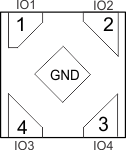
TPD4E6B06 po_new_slvsck3.gif

Pin Functions

PIN I/O DESCRIPTION
NO NAME
1 IO1 IO ESD protected line
2 IO2 IO ESD protected line
3 IO3 IO ESD protected line
4 IO4 IO ESD protected line
5 GND Ground