ZHCSCQ5C August 2014 – September 2017 TPD1E05U06-Q1 , TPD4E05U06-Q1
PRODUCTION DATA.
8 Application and Implementation
8.1 Application Information
The TPD4E05U06-Q1 is a diode type TVS which is typically used to provide a path to ground for dissipating ESD events on hi-speed signal lines between a human interface connector and a system. As the current from ESD passes through the TVS, only a small voltage drop is present across the diode. This is the voltage presented to the protected IC. The low RDYN of the triggered TVS holds this voltage, VCLAMP, to a safe level for the protected IC.
8.2 Typical Application
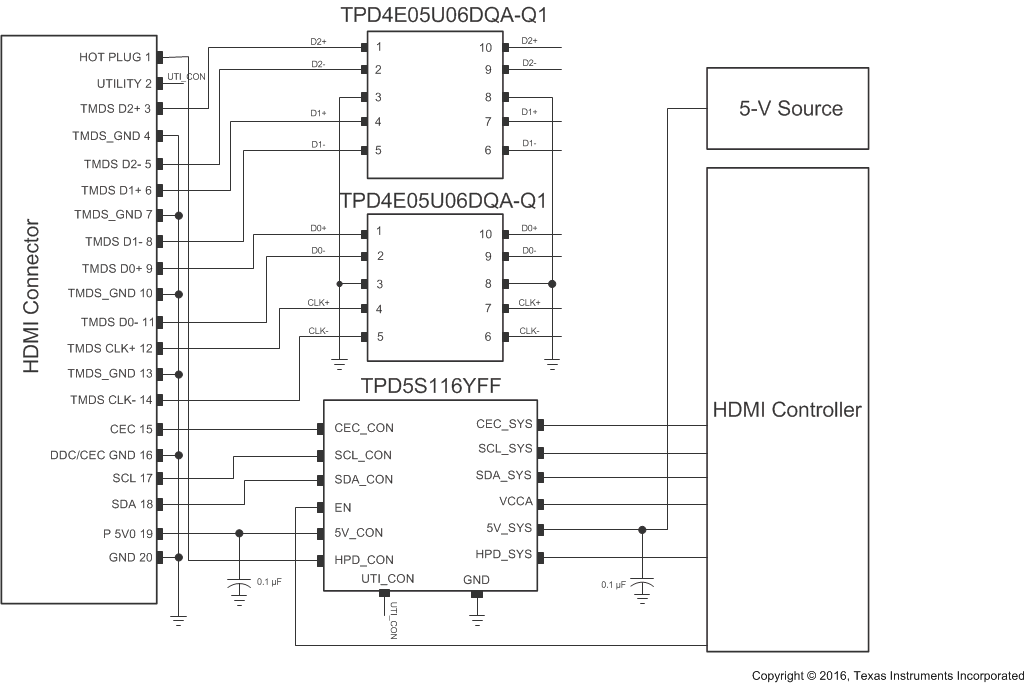
 Figure 11. HDMI 1.4 Application
8.2.1 Design Requirements
For this design example, two TPD4E05U06-Q1 devices, and a TPD5S116 are being used in an HDMI 1.4 application. This provides a complete port protection scheme.
Given the HDMI 1.4 application, the parameters in Table 1 are known.
Table 1. Design Parameters
| DESIGN PARAMETER | VALUE |
|---|---|
| Signal range on pins 1, 2, 4, or 5 | 0 V to 5 V |
| Operating frequency | 1.7 GHz |
8.2.2 Detailed Design Procedure
To begin the design process, some parameters must be decided upon; the designer needs to know the following:
- Signal range on all the protected lines
- Operating frequency
8.2.2.1 Signal Range on Pin 1, 2, 4, or 5
The TPD4E05U06-Q1 has 4 identical protection channels for signal lines. The symmetry of the device provides flexibility when selecting which of the 4 I/O channels protect which signal lines. Any I/O will support a signal range of 0 to 5.5 V.
8.2.2.2 Operating Frequency
The TPD4E05U06-Q1 has a capacitance of 0.5 pF (Typical), supporting HDMI 1.4 data rates.
8.2.3 Application Curve
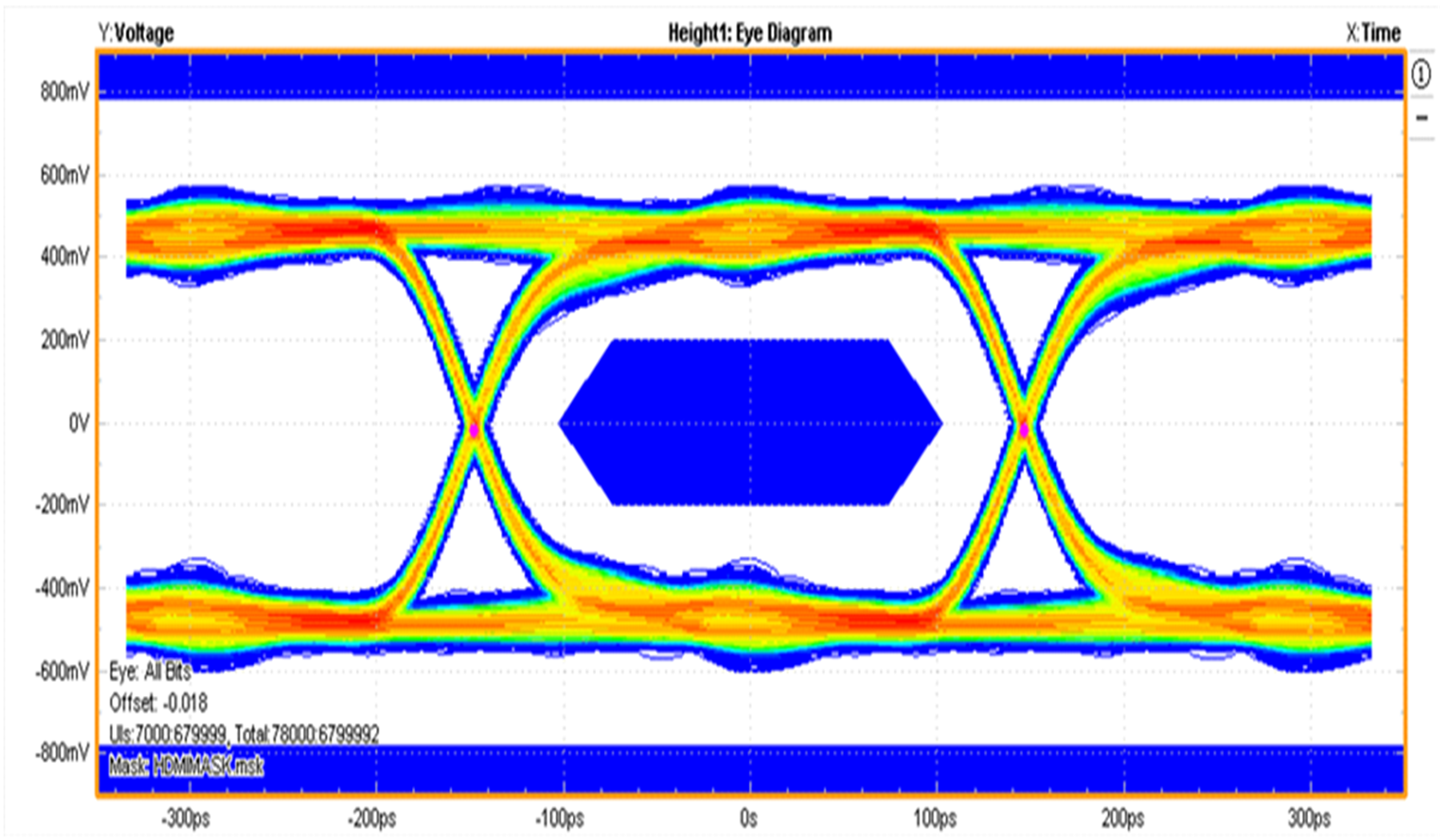
 Figure 12. 3.4 Gbps HDMI Eye Diagram