SLVS796I September   2008  – March 2016 TPD2E007

PRODUCTION DATA.  

  1. Features
  2. Applications
  3. Description
  4. Revision History
  5. Pin Configuration and Functions
  6. Specifications
    1. 6.1 Absolute Maximum Ratings
    2. 6.2 ESD Ratings
    3. 6.3 ESD Ratings: Surge Protection
    4. 6.4 Recommended Operating Conditions
    5. 6.5 Thermal Information
    6. 6.6 Electrical Characteristics
    7. 6.7 Typical Characteristics
  7. Detailed Description
    1. 7.1 Overview
    2. 7.2 Functional Block Diagram
    3. 7.3 Feature Description
      1. 7.3.1 IEC 61000-4-2 Level 4 ESD Protection
      2. 7.3.2 IEC 61000-4-5 Surge Protection
      3. 7.3.3 IO Capacitance
      4. 7.3.4 Low 50-nA Leakage Current
      5. 7.3.5 Space-Saving PicoStar and SOT Package
    4. 7.4 Device Functional Modes
  8. Application and Implementation
    1. 8.1 Application Information
    2. 8.2 Typical Application
      1. 8.2.1 Design Requirements
      2. 8.2.2 Detailed Design Procedure
        1. 8.2.2.1 Signal Range on IO1 and IO2 Pins
        2. 8.2.2.2 Surge Withstand
      3. 8.2.3 Application Curve
  9. Power Supply Recommendations
  10. 10Layout
    1. 10.1 Layout Guidelines
    2. 10.2 Layout Example
  11. 11Device and Documentation Support
    1. 11.1 Community Resources
    2. 11.2 Trademarks
    3. 11.3 Electrostatic Discharge Caution
    4. 11.4 Glossary
  12. 12Mechanical, Packaging, and Orderable Information

封装选项

机械数据 (封装 | 引脚)
散热焊盘机械数据 (封装 | 引脚)
订购信息

5 Pin Configuration and Functions

DCK Package
3-Pin SOT
Top View
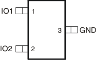
TPD2E007 po_dck_lvs796.gif


YFM Package
4-Pin PicoStar
Bottom View
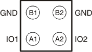
TPD2E007 po_lvs796.gif
0.8 mm × 0.8 mm (0.4 mm pitch)

Pin Functions

PIN I/O DESCRIPTION
NAME DCK
NO.
YFM
NO.
GND 3 B1, B2 G Ground
IO1 1 A1 IO ESD protected channel
IO2 2 A2 IO ESD protected channel