SLVS796I September 2008 – March 2016 TPD2E007
PRODUCTION DATA.
8 Application and Implementation
NOTE
Information in the following applications sections is not part of the TI component specification, and TI does not warrant its accuracy or completeness. TI’s customers are responsible for determining suitability of components for their purposes. Customers should validate and test their design implementation to confirm system functionality.
8.1 Application Information
TPD2E007 is a diode type TVS which is typically used to provide a path to ground for dissipating ESD events on signal lines between a human interface connector and a system. As the current from ESD passes through the TVS, only a small voltage drop is present across the diode. This is the voltage presented to the protected IC.
8.2 Typical Application
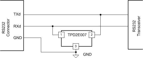
 Figure 6. Example Schematic
8.2.1 Design Requirements
For this design example, a single TPD2E007 is used to protect an RS232 3-wire connector.
Given the application, the following parameters are known.
Table 1. Design Parameters
| DESIGN PARAMETER | VALUE |
|---|---|
| Signal range on all pins except GND | –12 V to 12 V |
| Surge Withstand - IEC 61000-4-5 | 150 W |
8.2.2 Detailed Design Procedure
To begin the design process, some parameters must be decided upon; the designer needs to know the following:
- Signal voltage range on all protected lines
- Surge Withstand
8.2.2.1 Signal Range on IO1 and IO2 Pins
The TPD2E007 has 2 IO pins which can support up to ±13 V.
8.2.2.2 Surge Withstand
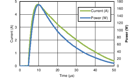
The TPD2E007 can withstand up to 170W of IEC 61000-4-5 8/20-µs surge.
8.2.3 Application Curve
 Figure 7. Surge Pulse Waveform