ZHCS790E March 2012 – December 2015 TPA3111D1-Q1
PRODUCTION DATA.
- 1 特性
- 2 应用
- 3 说明
- 4 修订历史记录
- 5 Pin Configuration and Functions
- 6 Specifications
- 7 Detailed Description
-
8 Application and Implementation
- 8.1 Application Information
- 8.2
Typical Application
- 8.2.1 Design Requirements
- 8.2.2
Detailed Design Procedure
- 8.2.2.1 Class-D Operation
- 8.2.2.2 TPA3111D1-Q1 Modulation Scheme
- 8.2.2.3 Ferrite Bead Filter Considerations
- 8.2.2.4 Efficiency: LC Filter Required With the Traditional Class-D Modulation Scheme
- 8.2.2.5 When to Use an Output Filter for EMI Suppression
- 8.2.2.6 Input Resistance
- 8.2.2.7 Input Capacitor, CI
- 8.2.2.8 BSN and BSP Capacitors
- 8.2.2.9 Differential Inputs
- 8.2.2.10 Using Low-ESR Capacitors
- 8.2.3 Application Curve
- 9 Power Supply Recommendations
- 10Layout
- 11器件和文档支持
- 12机械、封装和可订购信息
封装选项
请参考 PDF 数据表获取器件具体的封装图。
机械数据 (封装 | 引脚)
- PWP|28
散热焊盘机械数据 (封装 | 引脚)
- PWP|28
订购信息
7 Detailed Description
7.1 Overview
The TPA3111D1-Q1 device is AEC-Q100 qualified with temperature grade 1 (–40°C to 125°C), HBM ESD classification level H2, and CDM ESD classification level C2 (see the ESD Ratings table). This automotive audio amplifier also features several protection mechanisms as follows:
- DC-Current Detection:
- The TPA3111D1-Q1 device protects speakers from DC current by reporting a fault on the FAULT pin and turning the amplifier outputs to a Hi-Z state when a DC current is detected. The PVCC supply must be cycled to clear this fault.
- Short-Circuit Protection and Automatic Recovery:
- The TPA3111D1-Q1 device has short circuit protection from the output pins to VCC, GND, or to each other. If a short circuit is detected, it is reported on the FAULT pin and the amplifier outputs switch to a Hi-Z state. The fault can be cleared by cycling the SD pin.
- To recover automatically from this fault, connect the FAULT pin directly to the SD pin.
- Thermal Protection:
- When the die temperature exceeds 150°C (±15°C) the device enters the shutdown state and the amplifier outputs are disabled. The TPA3111D1-Q1 device recovers automatically when the temperature decreases by 15°C.
The functional modes of the TPA3111D1-Q1 device are as follows:
- Gain setting:
- The gain of the TPA3111D1-Q1 device is set to one of four options by the state of the GAIN0 and GAIN1 pins. Changing the gain setting also changes the input impedance of the TPA3111D1-Q1 device.
- Refer to Table 2 for a list of the gain settings.
- Shutdown Mode:
- The SD pin can be used to enter the shutdown mode which mutes the amplifier and causes the TPA3111D1-Q1 device to enter a low-current state. This mode can also be triggered to improve power-off pop performance.
- PLIMIT:
- The PLIMIT pin limits the output peak-to-peak voltage based on the voltage supplied to the PLIMIT pin. The peak output voltage is limited to four times the voltage at the PLIMIT pin.
The Feature Description and Device Functional Modes sections provide more details about these functions.
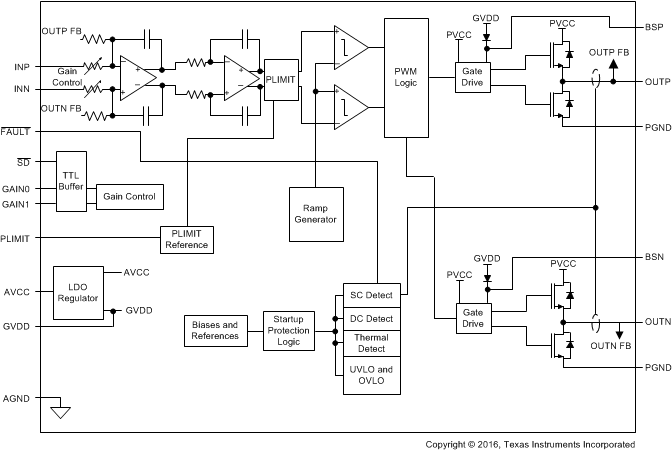
7.2 Functional Block Diagram

7.3 Feature Description
7.3.1 DC Detect
The TPA3111D1-Q1 circuitry protects the speakers from DC current which might occur because of defective capacitors on the input or shorts on the printed circuit board at the inputs. A DC-detect fault is reported on the FAULT pin as a low state. The DC-detect fault also causes the amplifier to shut down by changing the state of the outputs to Hi-Z. To clear the DC detect, cycle the PVCC supply. Cycling SD does NOT clear a DC-detect fault.
A DC-detect fault is issued when the output differential duty-cycle exceeds 14% (for example, 57%, –43%) for more than 420 ms at the same polarity. This feature helps protect the speaker from large DC currents or AC currents less than 2 Hz. To avoid nuisance faults because of the DC detect circuit, hold the SD pin low at power-up until the signals at the inputs are stable. Also, match the impedance at the positive and negative input to avoid nuisance DC-detect faults.
Table 1 lists the minimum differential input voltages required to trigger the DC detect. The inputs must remain at or above the voltage listed in the table for more than 420 ms to trigger the DC detect.
Table 1. DC Detect Threshold
| AV (dB) | VIN (mV, DIFFERENTIAL) |
|---|---|
| 20 | 112 |
| 26 | 56 |
| 32 | 28 |
| 36 | 17 |
7.3.2 Short-Circuit Protection and Automatic Recovery Feature
The TPA3110D2-Q1 device has protection from overcurrent conditions caused by a short circuit on the output stage. The short-circuit protection fault is reported on the FAULT pin as a low state. The amplifier outputs are switched to a Hi-Z state when the short circuit-protection latch is engaged. The latch is cleared by cycling the SD pin through the low state.
If automatic recovery from the short-circuit protection latch is desired, connect the FAULT pin directly to the SD pin. This allows the FAULT pin function to automatically drive the SD pin low, which clears the short-circuit protection latch.
7.3.3 Thermal Protection
Thermal protection on the TPA3111D1-Q1 device prevents damage to the device when the internal die temperature exceeds 150°C. This trip point has a ±15°C tolerance from device to device. When the die temperature exceeds the thermal set point, the device enters the shutdown state and the outputs are disabled. This is not a latched fault. The thermal fault is cleared once the temperature of the die is reduced by 15°C. The device begins normal operation at this point with no external system interaction.
Thermal protection faults are NOT reported on the FAULT pin.
7.3.4 GVDD Supply
The GVDD supply powers the gates of the output full bridge transistors. The GVDD supply can also supply the PLIMIT voltage divider circuit. Add a 1-μF capacitor to ground at this pin.
7.4 Device Functional Modes
7.4.1 Gain Setting Through Gain0 and Gain1 Inputs
The gain of the TPA3111D1-Q1 device is set by two input pins, GAIN0 and GAIN1. The voltage slew rate of these gain pins, along with pins 1 and 14, must be restricted to no more than 10 V/ms. For higher slew rates, use a 100-kΩ resistor in series with the pins.
The gains listed in Table 2 are realized by changing the taps on the input resistors inside the amplifier which causes the input impedance (ZI) to be dependent on the gain setting. The actual gain settings are controlled by ratios of resistors, so the gain variation from part-to-part is small. However, the input impedance from part-to-part at the same gain may shift by ±20% because of shifts in the actual resistance of the input resistors.
For design purposes, the input network (discussed in the Input Resistance section) should be designed assuming an input impedance of 7.2 kΩ, which is the absolute minimum input impedance of the TPA3111D1-Q1 device. At the lower gain settings, the input impedance could increase as high as 72 kΩ.
Table 2. Gain Setting
| GAIN1 | GAIN0 | AMPLIFIER GAIN (dB) | INPUT IMPEDANCE (kΩ) |
|---|---|---|---|
| TYPICAL | TYPICAL | ||
| 0 | 0 | 20 | 60 |
| 0 | 1 | 26 | 30 |
| 1 | 0 | 32 | 15 |
| 1 | 1 | 36 | 9 |
7.4.2 SD Operation
The TPA3111D1-Q1 device employs a shutdown mode of operation designed to reduce supply current (ICC) to the absolute minimum level during periods of non-use for power conservation. The SD input pin should be held high (see the AC Characteristics: VCC = 24 V and AC Characteristics: VCC = 12 V tables for the trip point values) during normal operation when the amplifier is in use. Pulling the SD pin low causes the outputs to mute and the amplifier to enter a low-current state. Never leave the SD pin unconnected. Amplifier operation is unpredictable if the SD pin is not connected.
For the best power-off pop performance, place the amplifier in the shutdown mode prior to removing the power supply voltage.
7.4.3 PLIMIT
The voltage at the PLIMIT pin (pin 10) can limit the power to levels below that which is possible based on the supply rail. Add a resistor divider from the GVDD pin to ground to set the voltage at the PLIMIT pin. An external reference can also be used if tighter tolerance is required. Also add a 1-μF capacitor from the PLIMIT pin to ground.
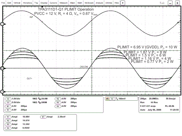
The PLIMIT circuit sets a limit on the output peak-to-peak voltage. This limit can be thought of as a virtual voltage rail, which is lower than the supply connected to PVCC. This virtual rail is four times the voltage at the PLIMIT pin. This output voltage can be used to calculate the maximum output power for a given maximum input voltage and speaker impedance.
 Figure 15. PLIMIT Circuit Operation
The PLIMIT circuits sets a limit on the output peak-to-peak voltage. The limiting occurs by limiting the duty cycle to the fixed maximum value. This limit can be thought of as a virtual voltage rail which is lower than the supply connected to PVCC. This virtual rail is four times the voltage at the PLIMIT pin. This output voltage can be used to calculate the maximum output power for a given maximum input voltage and speaker impedance. Use Equation 1 to calculate the maximum power output (POUT).

where
- RS is the total series resistance including RDS(on), and any resistance in the output filter.
- RL is the load resistance.
- VP is the peak amplitude of the output possible within the supply rail.
- VP = 4 × PLIMIT voltage if PLIMIT < 4 × VP
- POUT(10%THD) = 1.25 × POUT(unclipped)
Table 3. PLIMIT Typical Operation
| TEST CONDITIONS | PLIMIT VOLTAGE | OUTPUT POWER (W) | OUTPUT VOLTAGE AMPLITUDE (VP-P) |
|---|---|---|---|
| PVCC = 24 V, VIN = 1 VRMS, RL = 4 Ω, Gain = 20 dB |
1.92 | 10 | 15 |
| PVCC = 24 V, VIN = 1 VRMS, RL = 4 Ω, Gain = 20 dB |
1.24 | 5 | 10 |
| PVCC = 12 V, VIN = 1 VRMS, RL = 4 Ω, Gain = 20 dB |
1.75 | 10 | 15.3 |
| PVCC = 12 V, VIN = 1 VRMS, RL = 4 Ω, Gain = 20 dB |
1.20 | 5 | 10.3 |