ZHCS790E March 2012 – December 2015 TPA3111D1-Q1
PRODUCTION DATA.
- 1 特性
- 2 应用
- 3 说明
- 4 修订历史记录
- 5 Pin Configuration and Functions
- 6 Specifications
- 7 Detailed Description
-
8 Application and Implementation
- 8.1 Application Information
- 8.2
Typical Application
- 8.2.1 Design Requirements
- 8.2.2
Detailed Design Procedure
- 8.2.2.1 Class-D Operation
- 8.2.2.2 TPA3111D1-Q1 Modulation Scheme
- 8.2.2.3 Ferrite Bead Filter Considerations
- 8.2.2.4 Efficiency: LC Filter Required With the Traditional Class-D Modulation Scheme
- 8.2.2.5 When to Use an Output Filter for EMI Suppression
- 8.2.2.6 Input Resistance
- 8.2.2.7 Input Capacitor, CI
- 8.2.2.8 BSN and BSP Capacitors
- 8.2.2.9 Differential Inputs
- 8.2.2.10 Using Low-ESR Capacitors
- 8.2.3 Application Curve
- 9 Power Supply Recommendations
- 10Layout
- 11器件和文档支持
- 12机械、封装和可订购信息
封装选项
请参考 PDF 数据表获取器件具体的封装图。
机械数据 (封装 | 引脚)
- PWP|28
散热焊盘机械数据 (封装 | 引脚)
- PWP|28
订购信息
6 Specifications
6.1 Absolute Maximum Ratings
over operating free-air temperature range (unless otherwise noted)(1)| MIN | MAX | UNIT | |||
|---|---|---|---|---|---|
| VCC | Supply voltage | AVCC, PVCC | –0.3 | 30 | V |
| VI | Interface pin voltage | SD, FAULT,GAIN0, GAIN1, AVCC (2) | –0.3 | VCC + 0.3 V | V |
| < 10 | V/ms | ||||
| PLIMIT | –0.3 | GVDD + 0.3 | V | ||
| INN, INP | –0.3 | 6.3 | V | ||
| Continuous total power dissipation | See Thermal Information | ||||
| RL | Minimum load resistance | BTL | 3.2 | ||
| TA | Operating free-air temperature range | –40 | 125 | °C | |
| TJ | Operating junction temperature range(3) | –40 | 150 | °C | |
| Tstg | Storage temperature range | –65 | 150 | °C | |
(1) Stresses beyond those listed under absolute maximum ratings may cause permanent damage to the device. These are stress ratings only, and functional operations of the device at these or any other conditions beyond those indicated under recommended operating conditions is not implied. Exposure to absolute-maximum-rated conditions for extended periods may affect device reliability.
(2) The voltage slew rate of these pins must be restricted to no more than 10 V/ms. For higher slew rates, use a 100-kΩ resistor in series with the pins, per application note SLUA626.
(3) The TPA3111D1-Q1 incorporates an exposed thermal pad on the underside of the chip. This acts as a heatsink, and it must be connected to a thermally dissipating plane for proper power dissipation. Failure to do so may result in the device going into thermal protection shutdown. See TI Technical Brief SLMA002 for more information about using the PowerPAD.
6.2 ESD Ratings
| VALUE | UNIT | ||||
|---|---|---|---|---|---|
| V(ESD) | Electrostatic discharge | Human-body model (HBM), per AEC Q100-002(1) | ±4000 | V | |
| Charged-device model (CDM), per AEC Q100-011 | ±250 | ||||
| Machine model | ±200 | ||||
(1) AEC Q100-002 indicates that HBM stressing shall be in accordance with the ANSI/ESDA/JEDEC JS-001 specification.
6.3 Recommended Operating Conditions
over operating free-air temperature range (unless otherwise noted)6.4 Thermal Information
| THERMAL METRIC (1) | TPA3111D1-Q1 | UNIT | |
|---|---|---|---|
| PWP (HTSSOP) | |||
| 28 PINS | |||
| RθJA | Junction-to-ambient thermal resistance | 30.3 | °C/W |
| RθJC(top) | Junction-to-case (top) thermal resistance | 33.5 | °C/W |
| RθJB | Junction-to-board thermal resistance | 17.5 | °C/W |
| ψJT | Junction-to-top characterization parameter | 0.9 | °C/W |
| ψJB | Junction-to-board characterization parameter | 7.2 | °C/W |
| RθJC(bot) | Junction-to-case (bottom) thermal resistance | 0.9 | °C/W |
(1) For more information about traditional and new thermal metrics, see the Semiconductor and IC Package Thermal Metrics application report, SPRA953.
6.5 DC Characteristics: VCC = 24 V
TA = –40°C to 125°C, RL = 8 Ω (unless otherwise noted)6.6 DC Characteristics: VCC = 12 V
TA = –40°C to 125°C, RL = 8 Ω (unless otherwise noted)6.7 AC Characteristics: VCC = 24 V
TA = –40°C to 125°C, RL = 8 Ω (unless otherwise noted)6.8 AC Characteristics: VCC = 12 V
TA = –40°C to 125°C, RL = 8 Ω (unless otherwise noted)6.9 Typical Characteristics
All measurements taken at 1 kHz, unless otherwise noted, using the TPA3110D2EVM, which is available at ti.com.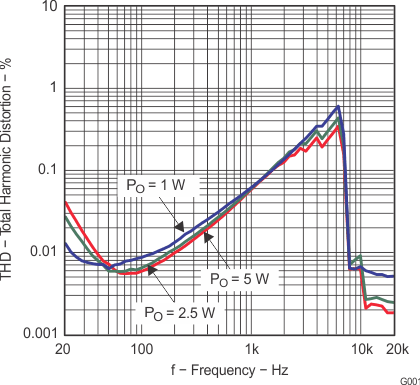
| Gain = 20 dB | VCC = 12 V | ZL = 8 Ω +66 µH |
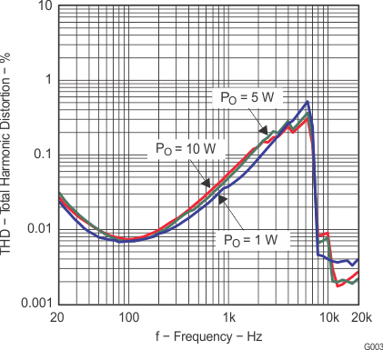
| Gain = 20 dB | VCC = 12 V | ZL = 4 Ω +33 µH |
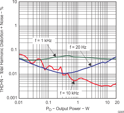
| Gain = 20 dB | VCC = 24 V | ZL = 8 Ω +66 µH |
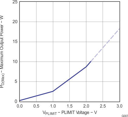
| Gain = 20 dB | VCC = 24 V | ZL = 8 Ω +66 µH |
| The dashed line represents thermally limited region. | ||
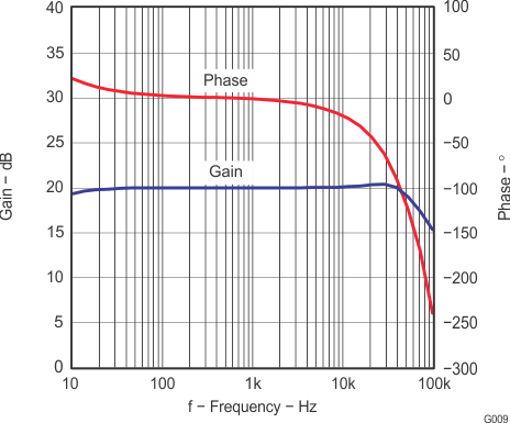
| Gain = 20 dB | VCC = 12 V | ZL = 8 Ω +66 µH |
| CI = 1 µF | VI = 0.1 VRMS | |
| Filter = Audio Precision AUX-0025 | ||
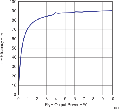
| Gain = 20 dB | VCC = 12 V | ZL = 4 Ω +33 µH |
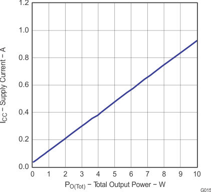
| Gain = 20 dB | VCC = 12 V | ZL = 4 Ω +33 µH |
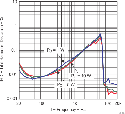
| Gain = 20 dB | VCC = 24 V | ZL = 8 Ω +66 µH |
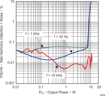
| Gain = 20 dB | VCC = 12 V | ZL = 8 Ω +66 µH |
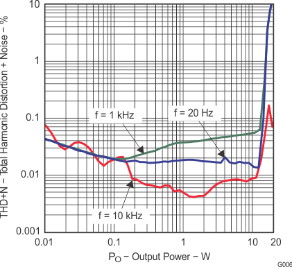
| Gain = 20 dB | VCC = 12 V | ZL = 4 Ω +33 µH |
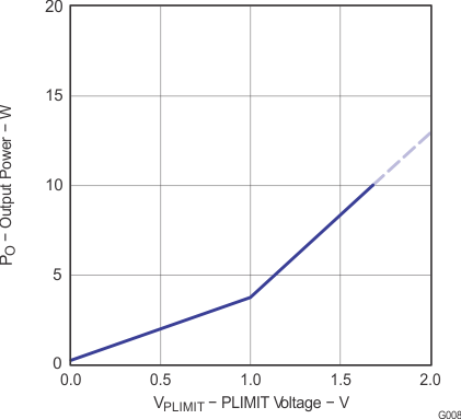
| Gain = 20 dB | VCC = 12 V | ZL = 4 Ω +33 µH |
| The dashed line represents thermally limited region. | ||
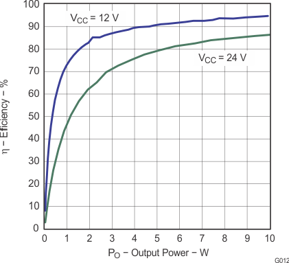
| Gain = 20 dB | ZL = 8 Ω +66 µH | |
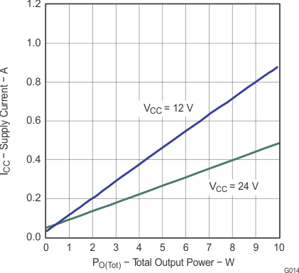
| Gain = 20 dB | ZL = 8 Ω +66 µH |
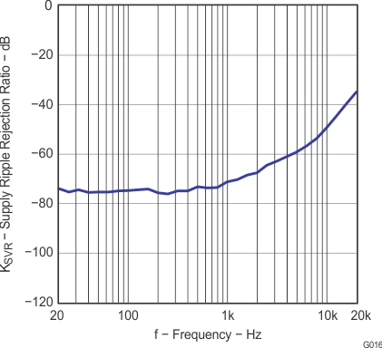
| Gain = 20 dB | VCC = 12 V | ZL = 8 Ω +66 µH |