ZHCSBS0C October 2013 – January 2015 TMS570LS3137-EP
PRODUCTION DATA.
- 1器件概述
- 2修订历史记录
- 3Device Comparison Table
-
4Pin Configuration and Functions
- 4.1
Pin Diagrams
- 4.1.1
Pin Attributes
- 4.1.1.1
GWT Package
- 4.1.1.1.1 Multi-Buffered Analog-to-Digital Converters (MibADC)
- 4.1.1.1.2 Enhanced High-End Timer Modules (N2HET)
- 4.1.1.1.3 General-Purpose Input / Output (GPIO)
- 4.1.1.1.4 FlexRay Interface Controller (FlexRay)
- 4.1.1.1.5 Controller Area Network Controllers (DCAN)
- 4.1.1.1.6 Local Interconnect Network Interface Module (LIN)
- 4.1.1.1.7 Standard Serial Communication Interface (SCI)
- 4.1.1.1.8 Inter-Integrated Circuit Interface Module (I2C)
- 4.1.1.1.9 Standard Serial Peripheral Interface (SPI)
- 4.1.1.1.10 Multi-Buffered Serial Peripheral Interface Modules (MibSPI)
- 4.1.1.1.11 Ethernet Controller
- 4.1.1.1.12 External Memory Interface (EMIF)
- 4.1.1.1.13 Embedded Trace Macrocell for Cortex-R4F CPU (ETM-R4F)
- 4.1.1.1.14 RAM Trace Port (RTP)
- 4.1.1.1.15 Data Modification Module (DMM)
- 4.1.1.1.16 System Module Interface
- 4.1.1.1.17 Clock Inputs and Outputs
- 4.1.1.1.18 Test and Debug Modules Interface
- 4.1.1.1.19 Flash Supply and Test Pads
- 4.1.1.1.20 No Connects
- 4.1.1.1.21 Supply for Core Logic: 1.2V nominal
- 4.1.1.1.22 Supply for I/O Cells: 3.3V nominal
- 4.1.1.1.23 Ground Reference for All Supplies Except VCCAD
- 4.1.1.1
GWT Package
- 4.1.1
Pin Attributes
- 4.1
Pin Diagrams
-
5Specifications
- 5.1 Absolute Maximum Ratings
- 5.2 ESD Ratings
- 5.3 Power-On Hours (POH)
- 5.4 Recommended Operating Conditions
- 5.5 Power Consumption
- 5.6 Thermal Data
- 5.7 Switching Characteristics
- 5.8 Wait States Required
- 5.9 I/O Electrical Characteristics
- 5.10 Output Buffer Drive Strengths
- 5.11 Input Timings
- 5.12 Output Timings
- 5.13 Low-EMI Output Buffers
-
6System Information and Electrical Specifications
- 6.1 Device Power Domains
- 6.2 Voltage Monitor Characteristics
- 6.3 Power Sequencing and Power On Reset
- 6.4 Warm Reset (nRST)
- 6.5 ARM© Cortex-R4F CPU Information
- 6.6 Clocks
- 6.7 Clock Monitoring
- 6.8 Glitch Filters
- 6.9 Device Memory Map
- 6.10 Flash Memory
- 6.11 Tightly-Coupled RAM Interface Module
- 6.12 Parity Protection for Peripheral RAMs
- 6.13 On-Chip SRAM Initialization and Testing
- 6.14 External Memory Interface (EMIF)
- 6.15 Vectored Interrupt Manager
- 6.16 DMA Controller
- 6.17 Real Time Interrupt Module
- 6.18 Error Signaling Module
- 6.19 Reset / Abort / Error Sources
- 6.20 Digital Windowed Watchdog
- 6.21
Debug Subsystem
- 6.21.1 Block Diagram
- 6.21.2 Debug Components Memory Map
- 6.21.3 JTAG Identification Code
- 6.21.4 Debug ROM
- 6.21.5 JTAG Scan Interface Timings
- 6.21.6 Advanced JTAG Security Module
- 6.21.7 Embedded Trace Macrocell (ETM-R4)
- 6.21.8 RAM Trace Port (RTP)
- 6.21.9 Data Modification Module (DMM)
- 6.21.10 Boundary Scan Chain
-
7Peripheral Information
- 7.1 Peripheral Legend
- 7.2 Multi-Buffered 12bit Analog-to-Digital Converter
- 7.3 General-Purpose Input/Output
- 7.4 Enhanced High-End Timer (N2HET)
- 7.5 FlexRay Interface
- 7.6 Controller Area Network (DCAN)
- 7.7 Local Interconnect Network Interface (LIN)
- 7.8 Serial Communication Interface (SCI)
- 7.9 Inter-Integrated Circuit (I2C)
- 7.10 Multi-Buffered / Standard Serial Peripheral Interface
- 7.11 Ethernet Media Access Controller
- 8Device and Documentation Support
- 9Mechanical, Packaging, and Orderable Information
8 Device and Documentation Support
8.1 Device and Development-Support Tool Nomenclature
To designate the stages in the product development cycle, TI assigns prefixes to the part numbers of all devices. Each commercial family member has one of three prefixes: TMX, TMP, or TMS (for example, TMS570LS3137). These prefixes represent evolutionary stages of product development from engineering prototypes (TMX) through fully qualified production devices/tools (TMS).
Device development evolutionary flow:
-
TMX Experimental device that is not necessarily representative of the final device's electrical specifications.
-
TMP Final silicon die that conforms to the device's electrical specifications but has not completed quality and reliability verification.
-
TMS Fully-qualified production device.
TMX and TMP devices are shipped against the following disclaimer:
"Developmental product is intended for internal evaluation purposes."
TMS devices have been characterized fully, and the quality and reliability of the device have been demonstrated fully. TI's standard warranty applies.
Predictions show that prototype devices (TMX or TMP) have a greater failure rate than the standard production devices. Texas Instruments recommends that these devices not be used in any production system because their expected end-use failure rate still is undefined. Only qualified production devices are to be used.
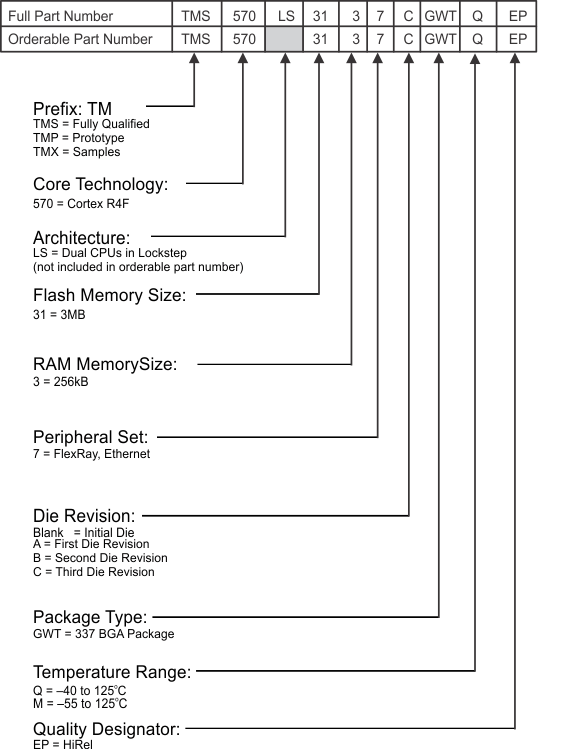 Figure 8-1 TMS570LS3137-EP Device Numbering Conventions
8.2 Documentation Support
8.2.1 Related Documentation from Texas Instruments
The following documents describe the TMS570LS3137-EP microcontroller.
| SPNU499 | TMS570LS31x/21x 16/32-Bit RISC Flash Microcontroller Technical Reference Manual details the integration, the environment, the functional description, and the programming models for each peripheral and subsytem in the device. | |||
| SPNZ195 | TMS570LS31x/21x Microcontroller Silicon Errata (Silicon Revision C) describes the known exceptions to the functional specifications for the device silicon revision(s). | |||
8.2.2 社区资源
下列链接提供到 TI 社区资源的连接。 链接的内容由各个分销商“按照原样”提供。 这些内容并不构成 TI 技术规范和标准且不一定反映 TI 的观点;请见 TI 的使用条款。
-
TI E2E™ 在线社区 TI 工程师对工程师 (E2E) 社区。 此社区的创建目的是为了促进工程师之间协作。 在 e2e.ti.com 中,您可以咨询问题、共享知识、探索思路,在同领域工程师的帮助下解决问题。
-
德州仪器 (TI) 嵌入式处理器维基网站 德州仪器 (TI) 嵌入式处理器维基网站。 此网站的建立是为了帮助开发人员从德州仪器 (TI) 的嵌入式处理器入门并且也为了促进与这些器件相关的硬件和软件的总体知识的创新和增长。
8.3 商标
E2E is a trademark of Texas Instruments.
Cortex is a trademark of ARM Limited.
ARM is a registered trademark of ARM Limited.
All other trademarks are the property of their respective owners.
8.4 静电放电警告

这些装置包含有限的内置 ESD 保护。 存储或装卸时,应将导线一起截短或将装置放置于导电泡棉中,以防止 MOS 门极遭受静电损伤。
8.6 Device Identification
8.6.1 Device Identification Code Register
The device identification code register identifies several aspects of the device including the silicon version. The details of the device identification code register are shown in Table 8-1. The device identification code register value for this device is:
- Rev A = 0x802AAD05
- Rev B = 0x802AAD15
- Rev C = 0x802AAD1D
| 31 | 30 | 29 | 28 | 27 | 26 | 25 | 24 |
| CP-15 | UNIQUE ID | ||||||
| R-1 | R-0000000 | ||||||
| 23 | 22 | 21 | 20 | 19 | 18 | 17 | 16 |
| UNIQUE ID | TECH | ||||||
| R-0010101 | R-0 | ||||||
| 15 | 14 | 13 | 12 | 11 | 10 | 9 | 8 |
| TECH | I/O VOLTAGE | PERIPH PARITY | FLASH ECC | RAM ECC | |||
| R-101 | R-0 | R-1 | R-10 | R-1 | |||
| 7 | 6 | 5 | 4 | 3 | 2 | 1 | 0 |
| VERSION | 1 | 0 | 1 | ||||
| R-00000 | R-1 | R-0 | R-1 | ||||
| LEGEND: R/W = Read/Write; R = Read only; -n = value after reset |
Table 8-1 Device ID Bit Allocation Register Field Descriptions
| Bit | Field | Value | Description |
|---|---|---|---|
| 31 | CP15 | Indicates the presence of coprocessor 15 | |
| 1 | CP15 present | ||
| 30-17 | UNIQUE ID | 10101 |
Silicon version (revision) bits. This bitfield holds a unique number for a dedicated device configuration (die). |
| 16-13 | TECH | Process technology on which the device is manufactured. | |
| 0101 | F021 | ||
| 12 | I/O VOLTAGE | I/O voltage of the device. | |
| 0 | I/O are 3.3v | ||
| 11 | PERIPHERAL PARITY | Peripheral Parity | |
| 1 | Parity on peripheral memories | ||
| 10-9 | FLASH ECC | Flash ECC | |
| 10 | Program memory with ECC | ||
| 8 | RAM ECC | Indicates if RAM memory ECC is present. | |
| 1 | ECC implemented | ||
| 7-3 | REVISION | Revision of the Device. | |
| 2-0 | 101 | The platform family ID is always 0b101 |
8.6.2 Die Identification Registers
The four die ID registers at addresses 0xFFFFE1F0, 0xFFFFE1F4, 0xFFFFE1F8 and FFFFE1FC form a 128-bit dieid with the information as shown in Table 8-2.
Table 8-2 Die-ID Registers
| Item | Number of Bits | Bit Location |
|---|---|---|
| X-coordinate on wafer | 12 | 0xFFFFE1F0[11:0] |
| Y-coordinate on wafer | 12 | 0xFFFFE1F0[23:12] |
| Wafer number | 8 | 0xFFFFE1F0[31:24] |
| Lot number | 24 | 0xFFFFE1F4[23:0] |
| Reserved | 72 | 0xFFFFE1F4[31:24], 0xFFFFE1F8[31:0], 0xFFFFE1FC[31:0] |
8.7 Module Certifications
The following communications modules have received certification of adherence to a standard.
FlexRay™ Certifications
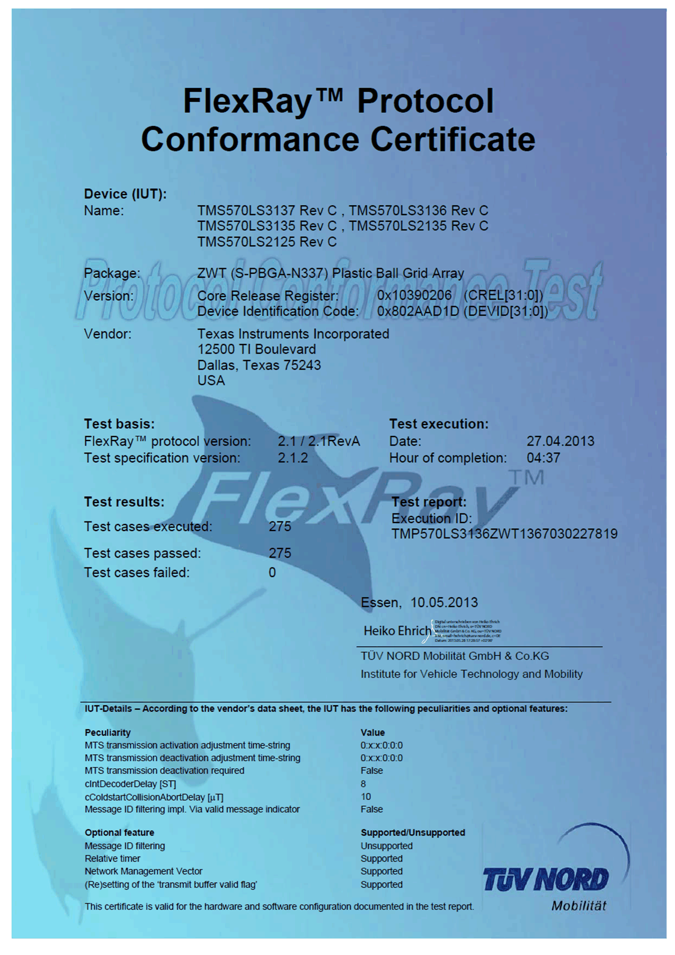 Figure 8-3 Flexray Certification for GWT Package
DCAN Certification
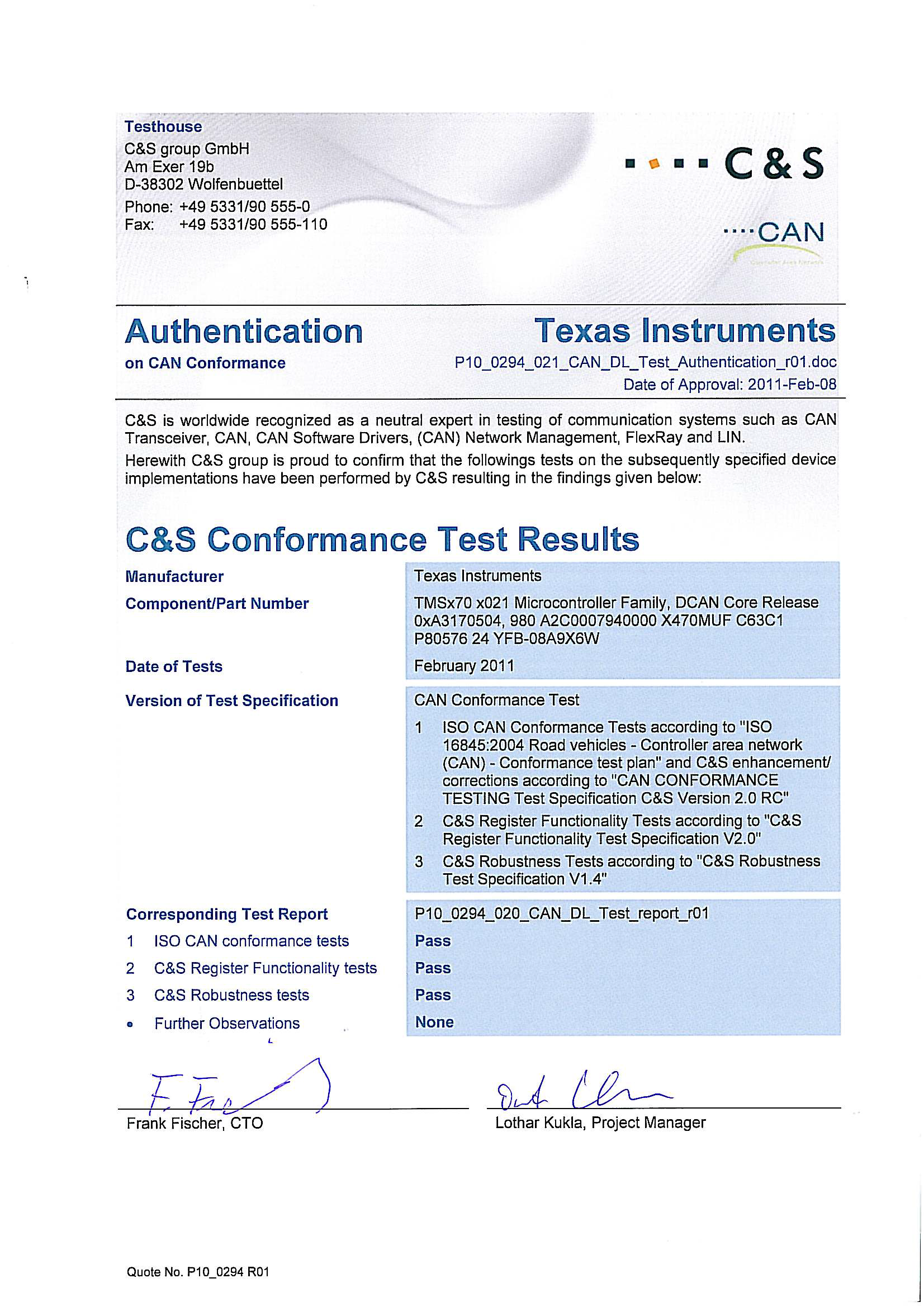 Figure 8-4 DCAN Certification