ZHCSCD3B April   2014  – August 2014 TMP75C

PRODUCTION DATA.  

  1. 特性
  2. 应用范围
  3. 说明
  4. 修订历史记录
  5. Pin Configuration and Functions
  6. Specifications
    1. 6.1 Absolute Maximum Ratings
    2. 6.2 Handling Ratings
    3. 6.3 Recommended Operating Conditions
    4. 6.4 Thermal Information
    5. 6.5 Electrical Characteristics
    6. 6.6 Typical Characteristics
  7. Detailed Description
    1. 7.1 Overview
    2. 7.2 Functional Block Diagram
    3. 7.3 Feature Description
      1. 7.3.1 Digital Temperature Output
      2. 7.3.2 Temperature Limits and Alert
      3. 7.3.3 Serial Interface
        1. 7.3.3.1 Bus Overview
        2. 7.3.3.2 Serial Bus Address
        3. 7.3.3.3 Writing and Reading Operation
        4. 7.3.3.4 Slave Mode Operations
          1. 7.3.3.4.1 Slave Receiver Mode:
          2. 7.3.3.4.2 Slave Transmitter Mode:
        5. 7.3.3.5 High-Speed (Hs) Mode
        6. 7.3.3.6 Timeout Function
        7. 7.3.3.7 Two-Wire Timing
        8. 7.3.3.8 Two-Wire Timing Diagrams
    4. 7.4 Device Functional Modes
      1. 7.4.1 Continuous-Conversion Mode
      2. 7.4.2 Shutdown Mode
      3. 7.4.3 One-Shot Mode
    5. 7.5 Programming
    6. 7.6 Register Map
  8. Application and Implementation
    1. 8.1 Application Information
    2. 8.2 Typical Application
      1. 8.2.1 Design Requirements
      2. 8.2.2 Detailed Design Procedure
      3. 8.2.3 Application Curves
  9. Power Supply Recommendations
  10. 10Layout
    1. 10.1 Layout Guidelines
    2. 10.2 Layout Example
  11. 11器件和文档支持
    1. 11.1 文档支持
      1. 11.1.1 相关文档 
    2. 11.2 Trademarks
    3. 11.3 Electrostatic Discharge Caution
    4. 11.4 术语表
  12. 12机械封装和可订购信息

封装选项

机械数据 (封装 | 引脚)
散热焊盘机械数据 (封装 | 引脚)
订购信息

10 Layout

10.1 Layout Guidelines

Place the power-supply bypass capacitor as close as possible to the supply and ground pins. The recommended value of this bypass capacitor is 0.01 μF. Additional decoupling capacitance can be added to compensate for noisy or high-impedance power supplies.

Pull up the open-drain output pins (SDA and ALERT) to a supply voltage rail (VS or higher but up to 3.6 V) through 10-kΩ pull-up resistors.

10.2 Layout Example

ai_recommended_layout_sbos706.gif
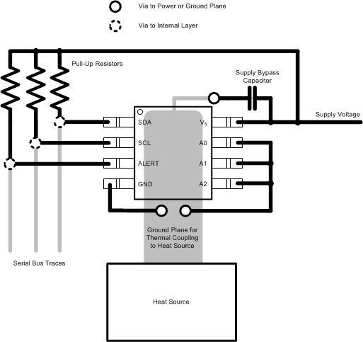
Figure 20. Layout Example