ZHCSCD2B April 2014 – August 2014 TMP75B
PRODUCTION DATA.
- 1 特性
- 2 应用范围
- 3 说明
- 4 修订历史记录
- 5 Pin Configuration and Functions
- 6 Specifications
-
7 Detailed Description
- 7.1 Overview
- 7.2 Functional Block Diagram
- 7.3
Feature Description
- 7.3.1 Digital Temperature Output
- 7.3.2 Temperature Limits and Alert
- 7.3.3 Serial Interface
- 7.4 Device Functional Modes
- 7.5 Programming
- 7.6 Register Map
- 8 Application and Implementation
- 9 Power Supply Recommendations
- 10Layout
- 11器件和文档支持
- 12机械封装和可订购信息
7 Detailed Description
7.1 Overview
The TMP75B is a digital temperature sensor optimal for thermal management and thermal protection applications. The TMP75B is two-wire and SMBus interface compatible, and is specified over a temperature range of –55°C to +125°C.
The temperature sensing device for the TMP75B is the chip itself. A bipolar junction transistor (BJT) inside the chip is used in a band-gap configuration to produce a voltage proportional to the chip temperature. The voltage is digitized and converted to a 12-bit temperature result in degrees Celsius, with a resolution of 0.0625°C. The package leads provide the primary thermal path because of the lower thermal resistance of the metal. Thus, the temperature result is equivalent to the local temperature of the printed circuit board (PCB) where the sensor is mounted.
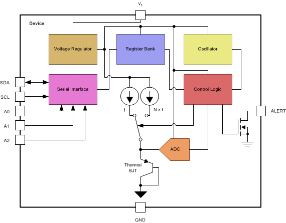
7.2 Functional Block Diagram
7.3 Feature Description
7.3.1 Digital Temperature Output
The 12-bit digital output from each temperature measurement conversion is stored in the read-only temperature register. Two bytes must be read to obtain the data, as shown in Figure 15. Note that byte 1 is the most significant byte, followed by byte 2, the least significant byte. The temperature result is left-justified with the 12 most significant bits used to indicate the temperature. There is no need to read the second byte if resolution below 1°C is not required. Table 1 summarizes the temperature data format. One LSB equals 0.0625°C. Negative numbers are represented in binary twos complement format.
Table 1. Temperature Data Format(1)
| TEMPERATURE (°C) | DIGITAL OUTPUT | |
|---|---|---|
| BINARY | HEX | |
| 128 | 0111 1111 1111 | 7FF |
| 127.9375 | 0111 1111 1111 | 7FF |
| 100 | 0110 0100 0000 | 640 |
| 80 | 0101 0000 0000 | 500 |
| 75 | 0100 1011 0000 | 4B0 |
| 50 | 0011 0010 0000 | 320 |
| 25 | 0001 1001 0000 | 190 |
| 0.25 | 0000 0000 0100 | 004 |
| 0 | 0000 0000 0000 | 000 |
| –0.25 | 1111 1111 1100 | FFC |
| –25 | 1110 0111 0000 | E70 |
| –55 | 1100 1001 0000 | C90 |
Table 1 does not supply a full list of all temperatures. Use the following rules to obtain the digital data format for a given temperature, and vice versa.
To convert positive temperatures to a digital data format:
Divide the temperature by the resolution. Then, convert the result to binary code with a 12-bit, left-justified format, and MSB = 0 to denote a positive sign.
Example: (+50°C) / (0.0625°C / LSB) = 800 = 320h = 0011 0010 0000
To convert a positive digital data format to temperature:
Convert the 12-bit, left-justified binary temperature result, with the MSB = 0 to denote a positive sign, to a decimal number. Then, multiply the decimal number by the resolution to obtain the positive temperature.
Example: 0011 0010 0000 = 320h = 800 × (0.0625°C / LSB) = +50°C
To convert negative temperatures to a digital data format:
Divide the absolute value of the temperature by the resolution, and convert the result to binary code with a 12-bit, left-justified format. Then, generate the twos complement of the result by complementing the binary number and adding one. Denote a negative number with MSB = 1.
Example: (|–25°C|) / (0.0625°C / LSB) = 400 = 190h = 0001 1001 0000
Two's complement format: 1110 0110 1111 + 1 = 1110 0111 0000
To convert a negative digital data format to temperature:
Generate the twos compliment of the 12-bit, left-justified binary number of the temperature result (with MSB = 1, denoting negative temperature result) by complementing the binary number and adding one. This represents the binary number of the absolute value of the temperature. Convert to decimal number and multiply by the resolution to get the absolute temperature, then multiply by –1 for the negative sign.
Example: 1110 0111 0000 has twos compliment of 0001 1001 0000 = 0001 1000 1111 + 1
Convert to temperature: 0001 1001 0000 = 190h = 400; 400 × (0.0625°C / LSB) = 25°C = (|–25°C|); (|–25°C|) × (–1) = –25°C
7.3.2 Temperature Limits and Alert
The temperature limits are stored in the TLOW and THIGH registers (Table 8 and Table 9) in the same format as the temperature result, and their values are compared to the temperature result on every conversion. The outcome of the comparison drives the behavior of the ALERT pin, which can operate as a comparator output or an interrupt, and is set by the TM bit in the configuration register (Table 7).
In comparator mode (TM = 0, default), the ALERT pin becomes active when the temperature is equal to or exceeds the value in THIGH (fault conditions) for a consecutive number of conversions as set by the FQ bits of the configuration register. ALERT clears when the temperature falls below TLOW for the same consecutive number of conversions. The difference between the two limits acts as a hysteresis on the comparator output, and a fault counter prevents false alerts as a result of environmental noise.
In interrupt mode (TM = 1), the ALERT pin becomes active when the temperature equals or exceeds the value in THIGH for a consecutive number of fault conditions. The ALERT pin remains active until a read operation of any register occurs, or the device successfully responds to the SMBus alert response address. The ALERT pin is also cleared if the device is placed in shutdown mode (see Shutdown Mode section for shutdown mode description). After the ALERT pin is cleared, this pin becomes active again only when the temperature falls below TLOW for a consecutive number of fault conditions, and remains active until cleared by a read operation of any register, or a successful response to the SMBus alert response address. After the ALERT pin is cleared, the cycle repeats with the ALERT pin becoming active when the temperature equals or exceeds THIGH, and so on. The ALERT pin can also be cleared by resetting the device with the general-call reset command. This action also clears the state of the internal registers in the device and the fault counter memory, returning the device to comparator mode (TM = 0).
The active state of the ALERT pin is set by the POL bit in the configuration register. When POL = 0 (default), the ALERT pin is active low. When POL = 1, the ALERT pin is active high. The operation of the ALERT pin in various modes is illustrated in Figure 7.
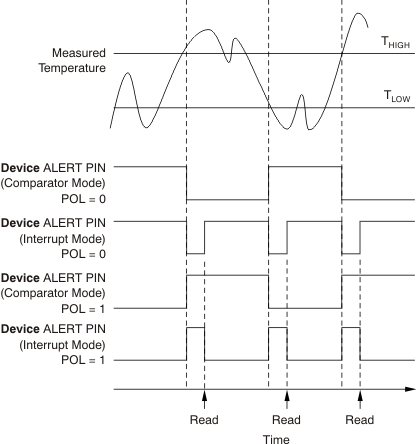 Figure 7. ALERT Pin Modes of Operation
7.3.3 Serial Interface
The TMP75B operates as a slave device only on the two-wire bus and SMBus. Connections to the bus are made using the open-drain I/O lines, SDA and SCL. The SDA and SCL pins feature integrated spike-suppression filters and Schmitt triggers to minimize the effects of input spikes and bus noise. The TMP75B supports the transmission protocol for both fast (1 kHz to 400 kHz) and high-speed (1 kHz to 3 MHz) modes. All data bytes are transmitted MSB first.
7.3.3.1 Bus Overview
The device that initiates the transfer is called a master, and the devices controlled by the master are slaves. The bus must be controlled by a master device that generates the serial clock (SCL), controls the bus access, and generates the start and stop conditions.
To address a specific device, initiate a start condition by pulling the data line (SDA) from a high to a low logic level while SCL is high. All slaves on the bus shift in the slave address byte; the last bit indicates whether a read or write operation follows. During the ninth clock pulse, the slave being addressed responds to the master by generating an acknowledge bit and pulling SDA low.
Data transfer is then initiated and sent over eight clock pulses followed by an acknowledge bit. During data transfer, SDA must remain stable while SCL is high because any change in SDA while SCL is high is interpreted as a start or stop signal.
After all data have been transferred, the master generates a stop condition indicated by pulling SDA from low to high, while SCL is high.
7.3.3.2 Serial Bus Address
To communicate with the TMP75B, the master must first communicate with slave devices using a slave address byte. The slave address byte consists of seven address bits, and a direction bit indicating the intent of executing either a read or write operation. The TMP75B features three address pins that allow up to eight devices to be addressed on a single bus. The TMP75B latches the status of the address pins at the start of a communication. Table 2 describes the pin logic levels and the corresponding address values.
Table 2. Address Pin Connections and Slave Addresses
| DEVICE TWO-WIRE ADDRESS | A2 | A1 | A0 |
|---|---|---|---|
| 1001000 | GND | GND | GND |
| 1001001 | GND | GND | VS |
| 1001010 | GND | VS | GND |
| 1001011 | GND | VS | VS |
| 1001100 | VS | GND | GND |
| 1001101 | VS | GND | VS |
| 1001110 | VS | VS | GND |
| 1001111 | VS | VS | VS |
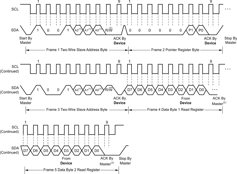
7.3.3.3 Writing and Reading Operation
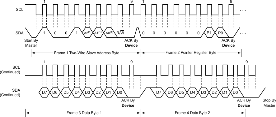
Accessing a particular register on the TMP75B is accomplished by writing the appropriate value to the pointer register. The value for the pointer register is the first byte transferred after the slave address byte with the R/W bit low. Every write operation to the TMP75B requires a value for the pointer register (see Figure 9).
When reading from the TMP75B, the last value stored in the pointer register by a write operation is used to determine which register is read by a read operation. To change the register pointer for a read operation, a new value must be written to the pointer register. This action is accomplished by issuing a slave address byte with the R/W bit low, followed by the pointer register byte. No additional data are required. The master can then generate a start condition and send the slave address byte with the R/W bit high to initiate the read command. See Figure 10 for details of this sequence. If repeated reads from the same register are desired, there is no need to continually send the pointer register bytes because the TMP75B stores the pointer register value until it is changed by the next write operation.
Note that register bytes are sent with the most significant byte first, followed by the least significant byte.
7.3.3.4 Slave-Mode Operations
The TMP75B can operate as a slave receiver or slave transmitter.
7.3.3.4.1 Slave Receiver Mode:
The first byte transmitted by the master is the slave address, with the R/W bit low. The TMP75B then acknowledges reception of a valid address. The next byte transmitted by the master is the pointer register. The TMP75B then acknowledges reception of the pointer register byte. The next byte or bytes are written to the register addressed by the pointer register. The TMP75B acknowledges reception of each data byte. The master can terminate data transfer by generating a start or stop condition.
7.3.3.4.2 Slave Transmitter Mode:
The first byte transmitted by the master is the slave address, with the R/W bit high. The slave acknowledges reception of a valid slave address. The next byte is transmitted by the slave and is the most significant byte of the register indicated by the pointer register. The master acknowledges reception of the data byte. The next byte transmitted by the slave is the least significant byte. The master acknowledges reception of the data byte. The master can terminate data transfer by generating a not-acknowledge bit on reception of any data byte, or by generating a start or stop condition.
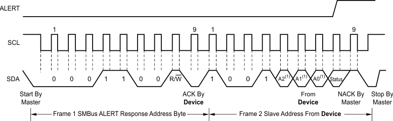
7.3.3.5 SMBus Alert Function
The TMP75B supports the SMBus alert function. When the TMP75B operates in interrupt mode (TM = 1), the ALERT pin may be connected as an SMBus alert signal. When a master senses that an alert condition is present on the ALERT line, the master sends an SMBus alert command (00011001) to the bus. If the ALERT pin is active, the device acknowledges the SMBus alert command and responds by returning its slave address on the SDA line. The eighth bit (LSB) of the slave address byte indicates whether the alert condition is caused by the temperature exceeding THIGH or falling below TLOW. The LSB is high if the temperature is greater than THIGH, or low if the temperature is less than TLOW. See Figure 11 for details of this sequence.
If multiple devices on the bus respond to the SMBus alert command, arbitration during the slave address portion of the SMBus alert command determines which device clears its alert status first. If the TMP75B wins the arbitration, its ALERT pin becomes inactive at the completion of the SMBus alert command. If the TMP75B loses the arbitration, its ALERT pin remains active.
7.3.3.6 General Call
The TMP75B responds to a two-wire general call address (0000000) if the eighth bit is 0. The device acknowledges the general call address and responds to commands in the second byte. If the second byte is 00000100, the TMP75B latches the status of the address pin, but does not reset. If the second byte is 00000110, the TMP75B internal registers are reset to power-up values.
7.3.3.7 High-Speed (Hs) Mode
In order for the two-wire bus to operate at frequencies above 400 kHz, the master device must issue an SMBus Hs-mode master code (00001xxx) as the first byte after a start condition to switch the bus to high-speed operation. The TMP75B does not acknowledge this byte, but does switch its input filters on SDA and SCL and its output filters on SDA to operate in Hs-mode, allowing transfers at up to 3 MHz. After the Hs-mode master code has been issued, the master transmits a two-wire slave address to initiate a data-transfer operation. The bus continues to operate in Hs-mode until a stop condition occurs on the bus. Upon receiving the stop condition, the TMP75B switches the input and output filters back to fast-mode operation.
7.3.3.8 Timeout Function
The TMP75B resets the serial interface if SCL or SDA are held low for 54 ms (typ) between a start and stop condition. If the TMP75B is pulled low, it releases the bus and then waits for a start condition. To avoid activating the timeout function, it is necessary to maintain a communication speed of at least 1 kHz for the SCL operating frequency.
7.3.3.9 Two-Wire Timing
The TMP75B is two-wire and SMBus compatible. Figure 8 to Figure 11 describe the various operations on the TMP75B. Parameters for Figure 8 are defined in Table 3. Bus definitions are:
-
Bus IdleBoth SDA and SCL lines remain high.
-
Start Data TransferA change in the state of the SDA line, from high to low, while the SCL line is high defines a start condition. Each data transfer is initiated with a start condition.
-
Stop Data TransferA change in the state of the SDA line from low to high while the SCL line is high defines a stop condition. Each data transfer is terminated with a repeated start or stop condition.
-
Data Transfer The number of data bytes transferred between a start and a stop condition is not limited, and is determined by the master device.
The receiver acknowledges the transfer of data. It is also possible to use the TMP75B for single-byte updates. To update only the MS byte, terminate communication by issuing a start or stop condition on the bus.
-
Acknowledge Each receiving device, when addressed, must generate an acknowledge bit.
A device that acknowledges must pull down the SDA line during the acknowledge clock pulse so that the SDA line is stable low during the high period of the acknowledge clock pulse. Setup and hold times must be taken into account. When a master receives data, the termination of the data transfer can be signaled by the master generating a not-acknowledge (1) on the last byte transmitted by the slave.
Table 3. Timing Diagram Requirements
| SYMBOL | PARAMETER | FAST MODE | HIGH-SPEED MODE | UNIT | |||
|---|---|---|---|---|---|---|---|
| MIN | MAX | MIN | MAX | ||||
| f(SCL) | SCL operating frequency | VS ≥ 1.8 V | 0.001 | 0.4 | 0.001 | 3 | MHz |
| VS < 1.8 V | 0.001 | 0.4 | 0.001 | 2.5 | MHz | ||
| t(BUF) | Bus free time between stop and start conditions | VS ≥ 1.8 V | 1300 | 160 | ns | ||
| VS < 1.8 V | 1300 | 260 | ns | ||||
| t(HDSTA) | Hold time after repeated start condition. After this period, the first clock is generated. |
600 | 160 | ns | |||
| t(SUSTA) | Repeated start condition setup time | 600 | 160 | ns | |||
| t(SUSTO) | Stop condition setup time | 600 | 160 | ns | |||
| t(HDDAT) | Data hold time | VS ≥ 1.8 V | 0 | 900 | 0 | 100 | ns |
| VS < 1.8 V | 0 | 900 | 0 | 140 | ns | ||
| t(SUDAT) | Data setup time | VS ≥ 1.8 V | 100 | 10 | ns | ||
| VS < 1.8 V | 100 | 20 | ns | ||||
| t(LOW) | SCL clock low period | VS ≥ 1.8 V | 1300 | 190 | ns | ||
| VS < 1.8 V | 1300 | 240 | ns | ||||
| t(HIGH) | SCL clock high period | 600 | 60 | ns | |||
| tR(SDA), tF(SDA) | Data rise and fall time | 300 | 80 | ns | |||
| tR(SCL), tF(SCL) | Clock rise and fall time | 300 | 40 | ns | |||
| tR | Clock and data rise time for SCLK ≤ 100 kHz | 1000 | ns | ||||
7.3.3.10 Two-Wire Timing Diagrams
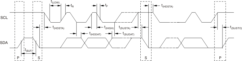 Figure 8. Two-Wire Timing Diagram
7.4 Device Functional Modes
7.4.1 Continuous-Conversion Mode
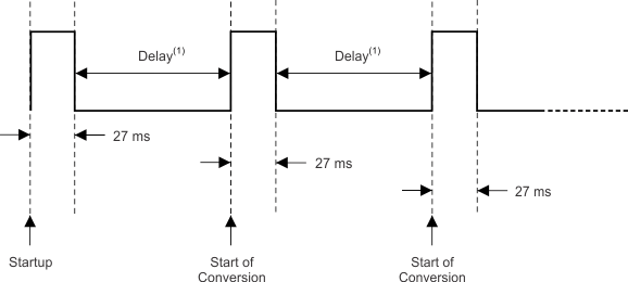
The default mode of the TMP75B is continuous conversion, where the ADC performs continuous temperature conversions and stores each result to the temperature register, overwriting the result from the previous conversion. Conversion rate bits CR1 and CR0 in the configuration register configure the TMP75B for typical conversion rates of 37 Hz, 18 Hz, 9 Hz, or 4 Hz. The TMP75B has a typical conversion time of 27 ms. To achieve different conversion rates, the TMP75B makes a conversion, and then powers down and waits for the appropriate delay set by CR1 and CR0. The default rate is 37 Hz (no delay between conversions).Table 4 shows the settings for CR1 and CR0.
Table 4. Conversion Rate Settings
| CR1 | CR0 | CONVERSION RATE (TYP) | IQ (TYP) |
|---|---|---|---|
| 0 | 0 | 37 Hz (continuous conversion, default) | 45 μA |
| 0 | 1 | 18 Hz | 22 μA |
| 1 | 0 | 9 Hz | 12 μA |
| 1 | 1 | 4 Hz | 6.5 μA |
After power-up or a general-call reset, the TMP75B immediately starts a conversion, as shown in Figure 12. The first result is available after 27 ms (typical). The active quiescent current during conversion is 45 μA (typical at +25°C). The quiescent current during delay is 1 μA (typical at +25°C).
7.4.2 Shutdown Mode
Shutdown mode saves maximum power by shutting down all device circuitry other than the serial interface, and reduces current consumption to typically less than 0.3 μA. Shutdown mode is enabled when the SD bit in the configuration register is set to 1; the device shuts down after the current conversion is completed. When SD is equal to 0, the device operates in continuous-conversion mode. When shutdown mode is enabled, the ALERT pin and fault counter clear in both comparator and interrupt modes; however, this clearing occurs with the rising edge of the shutdown signal. After shutdown is enabled, reprogramming shutdown does not clear the ALERT pin and the fault counter until a rising edge is generated on the shutdown signal.
7.4.3 One-Shot Mode
The TMP75B features a one-shot temperature measurement mode. When the device is in shutdown mode, writing a 1 to the OS bit starts a single temperature conversion. The device returns to the shutdown state at the completion of the single conversion. This mode reduces power consumption in the TMP75B when continuous temperature monitoring is not required. When the configuration register is read, the OS bit always reads zero.
7.5 Programming
Figure 13 shows the internal register structure of the TMP75B. Use the 8-bit pointer register to address a given data register. The pointer register uses the two LSBs to identify which of the data registers respond to a read or write command. Figure 14 identifies the bits of the pointer register byte.
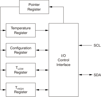 Figure 13. Internal Register Structure
7.6 Register Map
Table 5 describes the registers available in the TMP75B with their pointer addresses, followed by the description of the bits in each register.
Table 5. Register Map and Pointer Addresses
| P1 | P0 | REGISTER |
|---|---|---|
| 0 | 0 | Temperature register (read only, default) |
| 0 | 1 | Configuration register (read/write) |
| 1 | 0 | TLOW register (read/write) |
| 1 | 1 | THIGH register (read/write) |
| 7 | 6 | 5 | 4 | 3 | 2 | 1 | 0 |
| Reserved | P1 | P0 | |||||
| W-0h | W-0h | W-0h | |||||
| LEGEND: R/W = Read/Write; R = Read only; W = Write only; -n = value after reset |
| 15 | 14 | 13 | 12 | 11 | 10 | 9 | 8 |
| T11 | T10 | T9 | T8 | T7 | T6 | T5 | T4 |
| R-0h | |||||||
| 7 | 6 | 5 | 4 | 3 | 2 | 1 | 0 |
| T3 | T2 | T1 | T0 | Reserved | |||
| R-0h | R-0h | ||||||
| LEGEND: R/W = Read/Write; R = Read only; -n = value after reset |
Table 6. Temperature Register Description
| Name | Description |
|---|---|
| T11 to T4 | The 8 MSBs of the temperature result (resolution of 1°C) |
| T3 to T0 | The 4 LSBs of the temperature result (resolution of 0.0625°C) |
| 15 | 14 | 13 | 12 | 11 | 10 | 9 | 8 |
| OS | CR | FQ | POL | TM | SD | ||
| R/W-0h | R/W-0h | R/W-0h | R/W-0h | R/W-0h | R/W-0h | ||
| 7 | 6 | 5 | 4 | 3 | 2 | 1 | 0 |
| Reserved | |||||||
| R-FFh | |||||||
| LEGEND: R/W = Read/Write; R = Read only; -n = value after reset |
Table 7. Configuration Register Description
| Name | Description |
|---|---|
| OS | One-shot mode In shutdown (SD = 1), write 1 to start a conversion. OS always reads back 0. |
| CR | Conversion rate control CR = 0h: 37-Hz conversion rate (typ) (default) CR = 1h: 18-Hz conversion rate (typ) CR = 2h: 9-Hz conversion rate (typ) CR = 3h: 4-Hz conversion rate (typ) |
| FQ | Fault queue to trigger the ALERT pin FQ = 0h: 1 fault (default) FQ = 1h: 2 faults FQ = 2h: 4 faults FQ = 3h: 6 faults |
| POL | ALERT polarity control POL = 0: ALERT is active low (default) POL = 1: ALERT is active high |
| TM | ALERT thermostat mode control TM = 0: ALERT is in comparator mode (default) TM = 1: ALERT is in interrupt mode |
| SD | Shutdown control bit SD = 0: Device is in continuous conversion mode (default) SD = 1: Device is in shutdown mode |
| 15 | 14 | 13 | 12 | 11 | 10 | 9 | 8 |
| L11 | L10 | L9 | L8 | L7 | L6 | L5 | L4 |
| R/W-4Bh | |||||||
| 7 | 6 | 5 | 4 | 3 | 2 | 1 | 0 |
| L3 | L2 | L1 | L0 | Reserved | |||
| R/W-0h | R-0h | ||||||
| LEGEND: R/W = Read/Write; R = Read only; -n = value after reset |
Table 8. TLOW Register Description
| Name | Description |
|---|---|
| L11 to L4 | The 8 MSBs of the temperature low limit (resolution of 1°C) |
| L3 to L0 | The 4 LSBs of the temperature low limit (resolution of 0.0625°C) |
| 15 | 14 | 13 | 12 | 11 | 10 | 9 | 8 |
| H11 | H10 | H9 | H8 | H7 | H6 | H5 | H4 |
| R/W-50h | |||||||
| 7 | 6 | 5 | 4 | 3 | 2 | 1 | 0 |
| H3 | H2 | H1 | H0 | Reserved | |||
| R/W-0h | R-0h | ||||||
| LEGEND: R/W = Read/Write; R = Read only; -n = value after reset |
Table 9. THIGH Register Description
| Name | Description |
|---|---|
| H11 to H4 | The 8 MSBs of the temperature high limit (resolution of 1°C) |
| H3 to H0 | The 4 LSBs of the temperature high limit (resolution of 0.0625°C) |