ZHCSCD2B April 2014 – August 2014 TMP75B
PRODUCTION DATA.
- 1 特性
- 2 应用范围
- 3 说明
- 4 修订历史记录
- 5 Pin Configuration and Functions
- 6 Specifications
-
7 Detailed Description
- 7.1 Overview
- 7.2 Functional Block Diagram
- 7.3
Feature Description
- 7.3.1 Digital Temperature Output
- 7.3.2 Temperature Limits and Alert
- 7.3.3 Serial Interface
- 7.4 Device Functional Modes
- 7.5 Programming
- 7.6 Register Map
- 8 Application and Implementation
- 9 Power Supply Recommendations
- 10Layout
- 11器件和文档支持
- 12机械封装和可订购信息
6 Specifications
6.1 Absolute Maximum Ratings
over operating free-air temperature range (unless otherwise noted) (1)| MIN | MAX | UNIT | ||
|---|---|---|---|---|
| Supply voltage, VS | 4 | V | ||
| Input voltage | SDA, SCL, ALERT, A2, A1 | -0.3 | 4 | V |
| A0 | -0.3 | (VS) + 0.3 | V | |
| Sink current | SDA, ALERT | 10 | mA | |
| Operating junction temperature | -55 | 150 | °C | |
(1) Stresses beyond those listed under Absolute Maximum Ratings may cause permanent damage to the device. These are stress ratings only, which do not imply functional operation of the device at these or any other conditions beyond those indicated under Recommended Operating Conditions. Exposure to absolute-maximum-rated conditions for extended periods may affect device reliability.
6.2 Handling Ratings
| MIN | MAX | UNIT | |||
|---|---|---|---|---|---|
| Tstg | Storage temperature range | -60 | 150 | °C | |
| V(ESD) | Electrostatic discharge | Human body model (HBM), per ANSI/ESDA/JEDEC JS-001, all pins(1) | –2000 | 2000 | V |
| Charged device model (CDM), per JEDEC specification JESD22-C101, all pins(2) | –1000 | 1000 | |||
(1) JEDEC document JEP155 states that 500-V HBM allows safe manufacturing with a standard ESD control process.
(2) JEDEC document JEP157 states that 250-V CDM allows safe manufacturing with a standard ESD control process.
6.3 Recommended Operating Conditions
over operating free-air temperature range (unless otherwise noted)| MIN | NOM | MAX | UNIT | ||
|---|---|---|---|---|---|
| Supply voltage | 1.4 | 1.8 | 3.6 | V | |
| Operating free-air temperature, TA | -55 | 125 | °C | ||
6.4 Thermal Information
| THERMAL METRIC(1) | TMP75B | UNIT | ||
|---|---|---|---|---|
| D (SOIC) | DGK (VSSOP) | |||
| 8 PINS | 8 PINS | |||
| RθJA | Junction-to-ambient thermal resistance | 125.4 | 188.1 | °C/W |
| RθJC(top) | Junction-to-case (top) thermal resistance | 71.5 | 79.1 | |
| RθJB | Junction-to-board thermal resistance | 65.8 | 109.6 | |
| ψJT | Junction-to-top characterization parameter | 21.1 | 15.3 | |
| ψJB | Junction-to-board characterization parameter | 65.3 | 108 | |
| RθJC(bot) | Junction-to-case (bottom) thermal resistance | N/A | N/A | |
(1) For more information about traditional and new thermal metrics, see the IC Package Thermal Metrics application report, SPRA953.
6.5 Electrical Characteristics
At TA = –55°C to +125°C and VS = +1.4 V to +3.6 V, unless otherwise noted. Typical values at TA = 25°C and VS = +1.8 V.| PARAMETER | TEST CONDITIONS | MIN | TYP | MAX | UNIT | |
|---|---|---|---|---|---|---|
| TEMPERATURE INPUT | ||||||
| Temperature range | –55 | +125 | °C | |||
| Temperature resolution | 0.0625 | °C | ||||
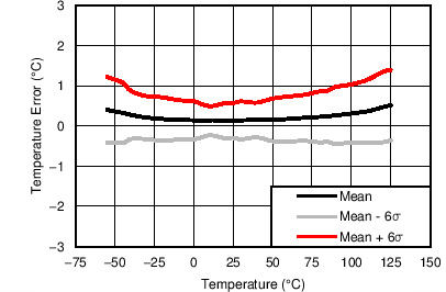
| Temperature accuracy (error) | –20°C to +85°C | ±0.5 | ±2 | °C | ||
| –55°C to +125°C | ±1 | ±3 | °C | |||
| DIGITAL INPUT/OUTPUT | ||||||
| VIH | High-level input voltage | 0.7(VS) | VS | V | ||
| VIL | Low-level input voltage | -0.3 | 0.3(VS) | V | ||
| IIN | Input current | 0 V < VIN < (VS) + 0.3 V | 1 | μA | ||
| VOL | Low-level output voltage | VS ≥ 2 V, IOUT = 3 mA | 0.4 | V | ||
| VS < 2 V, IOUT = 3 mA | 0.2(VS) | V | ||||
| ADC resolution | 12 | Bit | ||||
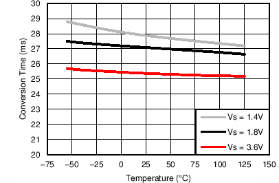
| Conversion time | One-shot mode | 20 | 27 | 35 | ms | |
| Conversion modes | CR1 = 0, CR0 = 0 (default) | 37 | Conv/s | |||
| CR1 = 0, CR0 = 1 | 18 | Conv/s | ||||
| CR1 = 1, CR0 = 0 | 9 | Conv/s | ||||
| CR1 = 1, CR0 = 1 | 4 | Conv/s | ||||
| Timeout time | 38 | 54 | 70 | ms | ||
| POWER SUPPLY | ||||||
| Operating supply range | 1.4 | 3.6 | V | |||
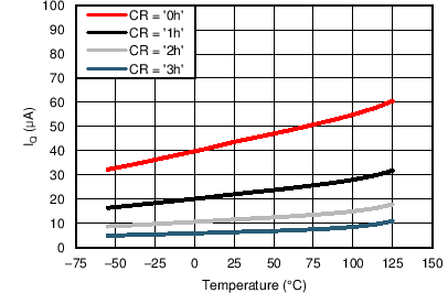
| IQ | Quiescent current | Serial bus inactive, CR1 = 0, CR0 = 0 (default) | 45 | 89 | μA | |
| Serial bus inactive, CR1 = 0, CR0 = 1 | 22 | 48 | μA | |||
| Serial bus inactive, CR1 = 1, CR0 = 0 | 12 | 30 | μA | |||
| Serial bus inactive, CR1 = 1, CR0 = 1 | 6.5 | 21 | μA | |||
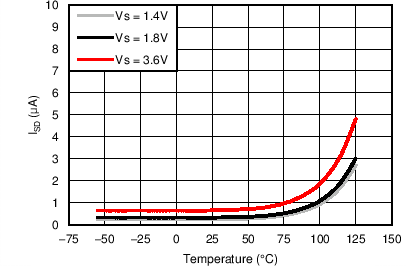
| ISD | Shutdown current | Serial bus inactive | 0.3 | 8 | μA | |
| Serial bus active, SCL frequency = 400 kHz | 10 | μA | ||||
| Serial bus active, SCL frequency = 3.4 MHz | 80 | μA | ||||
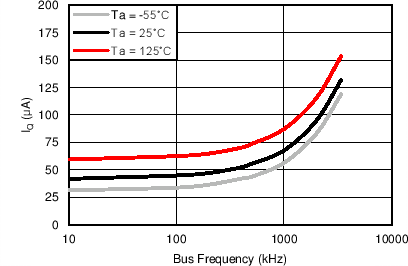
6.6 Typical Characteristics
At TA = 25°C and VS = +1.8 V (unless otherwise noted).