ZHCSB68A June 2013 – December 2014 TMP451
PRODUCTION DATA.
- 1 特性
- 2 应用
- 3 说明
- 4 修订历史记录
- 5 Pin Configuration and Functions
- 6 Specifications
-
7 Detailed Description
- 7.1 Overview
- 7.2 Functional Block Diagram
- 7.3 Feature Description
- 7.4 Device Functional Modes
- 7.5 Programming
- 7.6
Register Map
- 7.6.1
Register Information
- 7.6.1.1 Pointer Register
- 7.6.1.2 Temperature Registers
- 7.6.1.3 Local Temperature High Byte Register (offset: Read = 00h; Write = N/A) [reset = 00h]
- 7.6.1.4 Remote Temperature High Byte Register (offset: Read = 01h; Write = N/A) [reset = 00h]
- 7.6.1.5 Status Register (offset: Read = 02h; Write = N/A) [reset = N/A]
- 7.6.1.6 Configuration Register (offset: Read = 03h; Write = 09h) [reset = 00h]
- 7.6.1.7 Conversion Rate Register (offset: Read = 04h; Write = 0Ah) [reset = 08h]
- 7.6.1.8 Local Temperature High Limit Register (offset: Read = 05h; Write = 0Bh) [reset = 55h]
- 7.6.1.9 Local Temperature Low Limit Register (offset: Read = 06h; Write = 0Ch) [reset = 00h]
- 7.6.1.10 Remote Temperature High Limit High Byte Register (offset: Read = 07h; Write = 0Dh) [reset = 55h]
- 7.6.1.11 Remote Temperature Low Limit High Byte Register (offset: Read = 08h; Write = 0Eh) [reset = 00h]
- 7.6.1.12 One-shot Start Register (offset: Read = N/A; Write = 0Fh) [reset = N/A]
- 7.6.1.13 Remote Temperature Low Byte Register (offset: Read = 10h; Write = N/A) [reset = 00h]
- 7.6.1.14 Remote Temperature Offset High Byte Register (offset: Read = 11h; Write = 11h) [reset = 00h]
- 7.6.1.15 Remote Temperature Offset Low Byte Register (offset: Read = 12h; Write = 12h) [reset = 00h]
- 7.6.1.16 Remote Temperature High Limit Low Byte Register (offset: Read = 13h; Write = 13h) [reset = 00h]
- 7.6.1.17 Remote Temperature Low Limit Low Byte Register (offset: Read = 14h; Write = 14h) [reset = 00h]
- 7.6.1.18 Local Temperature Low Byte Register (offset: Read = 15h; Write = N/A) [reset = 00h]
- 7.6.1.19 Remote Temperature THERM Limit Register (offset: Read = 19h; Write = 19h) [reset = 6C]
- 7.6.1.20 Local Temperature THERM Limit Register (offset: Read = 20h; Write = 20h) [reset = 55]
- 7.6.1.21 THERM Hysteresis Register (offset: Read = 21h; Write = 21h) [reset = 0Ah]
- 7.6.1.22 Consecutive ALERT Register (offset: Read = 22h; Write = 22h) [reset = 01h]
- 7.6.1.23 η-Factor Correction Register (offset: Read = 23h; Write = 23h) [reset = 00h]
- 7.6.1.24 Digital Filter Control Register (offset: Read = 24h; Write = 24h) [reset = 00h]
- 7.6.1.25 Manufacturer ID Register (offset: Read = FEh; Write = N/A) [reset = 55]
- 7.6.1
Register Information
- 8 Application and Implementation
- 9 Power Supply Recommendations
- 10Layout
- 11器件和文档支持
- 12机械封装和可订购信息
6 Specifications
6.1 Absolute Maximum Ratings
Over operating free-air temperature range, unless otherwise noted.(1)| MIN | MAX | UNIT | ||
|---|---|---|---|---|
| Power supply | V+ | –0.3 | 3.6 | V |
| Input voltage | THERM, ALERT/THERM2, SDA and SCL only | –0.3 | 3.6 | V |
| D+ only | –0.3 | (V+) + 0.3 | V | |
| D– only | –0.3 | 0.3 | V | |
| Input current | 10 | mA | ||
| Operating temperature | –55 | 127 | °C | |
| Junction temperature (TJmax) | 150 | °C | ||
| Tstg | Storage temperature | –60 | 150 | °C |
(1) Stresses above these ratings may cause permanent damage. Exposure to absolute maximum conditions for extended periods may degrade device reliability. These are stress ratings only, and functional operation of the device at these or any other conditions beyond those specified is not implied.
6.2 ESD Ratings
| VALUE | UNIT | ||||
|---|---|---|---|---|---|
| V(ESD) | Electrostatic discharge | Human body model (HBM), per ANSI/ESDA/JEDEC JS-001, all pins(1) | ±2000 | V | |
| Charged device model (CDM), per JEDEC specification JESD22-C101, all pins(2) | ±750 | ||||
(1) JEDEC document JEP155 states that 500-V HBM allows safe manufacturing with a standard ESD control process.
(2) JEDEC document JEP157 states that 250-V CDM allows safe manufacturing with a standard ESD control process.
6.3 Recommended Operating Conditions
over operating free-air temperature range (unless otherwise noted)| MIN | NOM | MAX | UNIT | ||
|---|---|---|---|---|---|
| Supply voltage | 1.7 | 3.3 | 3.6 | V | |
| TA | Operating free-air temperature | –40 | 125 | °C | |
6.4 Thermal Information
| THERMAL METRIC(1) | TMP451 | UNIT | |
|---|---|---|---|
| DQF | |||
| 8 PINS | |||
| RθJA | Junction-to-ambient thermal resistance | 171.3 | °C/W |
| RθJC(top) | Junction-to-case (top) thermal resistance | 81.4 | |
| RθJB | Junction-to-board thermal resistance | 137.9 | |
| ψJT | Junction-to-top characterization parameter | 3.9 | |
| ψJB | Junction-to-board characterization parameter | 140 | |
(1) For more information about traditional and new thermal metrics, see the IC Package Thermal Metrics application report, SPRA953.
6.5 Electrical Characteristics
At TA = –40°C to 125°C and V+ = 3.3 V, unless otherwise noted.| PARAMETER | CONDITIONS | MIN | TYP | MAX | UNIT | ||
|---|---|---|---|---|---|---|---|
| TEMPERATURE ERROR | |||||||
| TELOCAL | Local temperature sensor | TA = 0°C to 70°C | ±0.25 | ±1 | °C | ||
| TA = –40°C to 125°C | ±1 | ±2 | °C | ||||
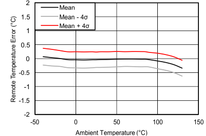
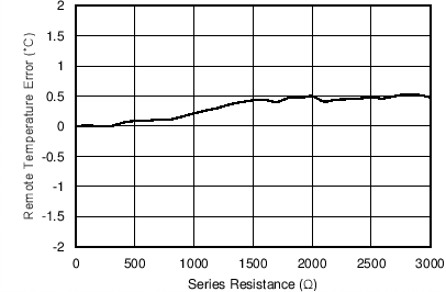
| TEREMOTE | Remote temperature sensor(1) | TA = 0°C to 70°C, TD = –55°C to 150°C | ±0.25 | ±1 | °C | ||
| TA = –40°C to 100°C, TD = –55°C to 150°C | ±1 | ±2 | °C | ||||
| TA = –40°C to 125°C, TD = –55°C to 150°C | ±2 | ±4 | °C | ||||
| Remote temperature sensor versus supply (local or remote) | V+ = 1.7 V to 3.6 V | ±0.1 | ±0.25 | °C/V | |||
| TEMPERATURE MEASUREMENT | |||||||
| Conversion time | One-Shot mode, local and remote total | 31 | 34 | ms | |||
| Local temperature sensor resolution | 12 | Bits | |||||
| Remote temperature sensor resolution | 12 | Bits | |||||
| Remote sensor source current, high | Series resistance 1 kΩ max | 120 | μA | ||||
| Remote sensor source current, medium | 45 | μA | |||||
| Remote sensor source current, low | 7.5 | μA | |||||
| η | Remote transistor ideality factor | TMP451 optimized ideality factor | 1.008 | ||||
| SMBus INTERFACE | |||||||
| VIH | High-level input voltage | 1.4 | V | ||||
| VIL | Low-level input voltage | 0.45 | V | ||||
| Hysteresis | 200 | mV | |||||
| SMBus output low sink current | 6 | mA | |||||
| VOL | Low-level output voltage | IO = 6 mA | 0.15 | 0.4 | V | ||
| Logic input current | 0 V ≤ VI ≤ 3.6 V | –1 | 1 | μA | |||
| SMBus input capacitance | 3 | pF | |||||
| SMBus clock frequency | 0.01 | 2.5 | MHz | ||||
| SMBus time-out | 20 | 25 | 30 | ms | |||
| SCL falling edge to SDA valid time | 1 | μs | |||||
| DIGITAL OUTPUTS (THERM, ALERT/THERM2) | |||||||
| VOL | Low-level output voltage | IO = 6 mA | 0.15 | 0.4 | V | ||
| IOH | High-level output leakage current | VO = V+ | 1 | μA | |||
| POWER SUPPLY | |||||||
| V(V+) | Specified voltage range | 1.7 | 3.6 | V | |||
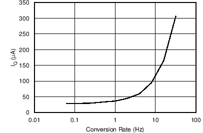
| IQ | Quiescent current | 0.0625 conversions per second | 27 | 40 | μA | ||
| 16 conversions per second | 165 | 250 | μA | ||||
| 32 conversions per second | 300 | 450 | μA | ||||
| Serial bus inactive, shutdown mode | 3 | 8 | μA | ||||
| Serial bus active, ƒS = 400 kHz, shutdown mode | 90 | μA | |||||
| Serial bus active, ƒS = 2.5 MHz, shutdown mode | 350 | μA | |||||
| POR | Power-on reset threshold | 1.2 | 1.55 | V | |||
(1) Tested with less than 5-Ω effective series resistance and 100-pF differential input capacitance.
6.6 Timing Requirements
| PARAMETER | FAST MODE | HIGH-SPEED MODE | UNIT | ||||||
|---|---|---|---|---|---|---|---|---|---|
| MIN | TYP | MAX | MIN | TYP | MAX | ||||
| ƒ(SCL) | SCL operating frequency | 0.001 | 0.4 | 0.001 | 2.5 | MHz | |||
| t(BUF) | Bus free time between STOP and START Condition | 1300 | 260 | ns | |||||
| t(HDSTA) | Hold time after repeated START condition. After this period, the first clock is generated. | 600 | 160 | ns | |||||
| t(SUSTA) | Repeated START condition setup time | 600 | 160 | ns | |||||
| t(SUSTO) | STOP condition setup time | 600 | 160 | ns | |||||
| t(HDDAT) | Data hold time | 0 | 900 | 0 | 150 | ns | |||
| t(SUDAT) | Data setup time | 100 | 30 | ns | |||||
| t(LOW) | SCL clock LOW period | 1300 | 260 | ns | |||||
| t(HIGH) | SCL clock HIGH period | 600 | 60 | ns | |||||
| tF, tR – SDA | Data fall and rise time | 300 | 80 | ns | |||||
| tF, tR – SCL | Clock fall and rise time | 300 | 40 | ns | |||||
| tR | Rise time for SCL ≤ 100 kHz | 1000 | ns | ||||||
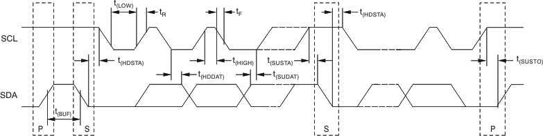 Figure 1. Two-Wire Timing Diagram
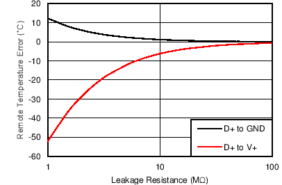
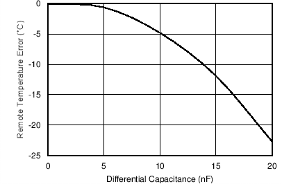
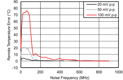
6.7 Typical Characteristics
At TA = 25°C and V+ = 3.3 V, unless otherwise noted.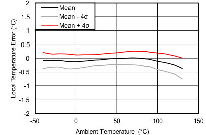
(At Default Conversion Rate of 16 Conversions per Second)
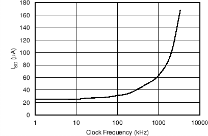
vs SCL Clock Frequency
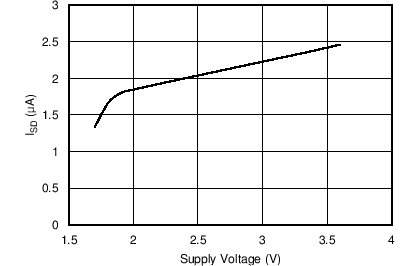
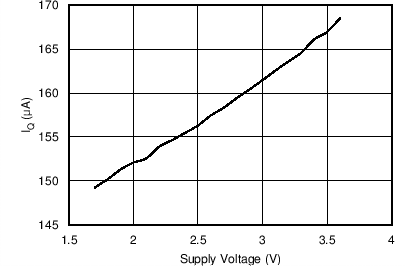
vs Supply Voltage