ZHCSB68A June 2013 – December 2014 TMP451
PRODUCTION DATA.
- 1 特性
- 2 应用
- 3 说明
- 4 修订历史记录
- 5 Pin Configuration and Functions
- 6 Specifications
-
7 Detailed Description
- 7.1 Overview
- 7.2 Functional Block Diagram
- 7.3 Feature Description
- 7.4 Device Functional Modes
- 7.5 Programming
- 7.6
Register Map
- 7.6.1
Register Information
- 7.6.1.1 Pointer Register
- 7.6.1.2 Temperature Registers
- 7.6.1.3 Local Temperature High Byte Register (offset: Read = 00h; Write = N/A) [reset = 00h]
- 7.6.1.4 Remote Temperature High Byte Register (offset: Read = 01h; Write = N/A) [reset = 00h]
- 7.6.1.5 Status Register (offset: Read = 02h; Write = N/A) [reset = N/A]
- 7.6.1.6 Configuration Register (offset: Read = 03h; Write = 09h) [reset = 00h]
- 7.6.1.7 Conversion Rate Register (offset: Read = 04h; Write = 0Ah) [reset = 08h]
- 7.6.1.8 Local Temperature High Limit Register (offset: Read = 05h; Write = 0Bh) [reset = 55h]
- 7.6.1.9 Local Temperature Low Limit Register (offset: Read = 06h; Write = 0Ch) [reset = 00h]
- 7.6.1.10 Remote Temperature High Limit High Byte Register (offset: Read = 07h; Write = 0Dh) [reset = 55h]
- 7.6.1.11 Remote Temperature Low Limit High Byte Register (offset: Read = 08h; Write = 0Eh) [reset = 00h]
- 7.6.1.12 One-shot Start Register (offset: Read = N/A; Write = 0Fh) [reset = N/A]
- 7.6.1.13 Remote Temperature Low Byte Register (offset: Read = 10h; Write = N/A) [reset = 00h]
- 7.6.1.14 Remote Temperature Offset High Byte Register (offset: Read = 11h; Write = 11h) [reset = 00h]
- 7.6.1.15 Remote Temperature Offset Low Byte Register (offset: Read = 12h; Write = 12h) [reset = 00h]
- 7.6.1.16 Remote Temperature High Limit Low Byte Register (offset: Read = 13h; Write = 13h) [reset = 00h]
- 7.6.1.17 Remote Temperature Low Limit Low Byte Register (offset: Read = 14h; Write = 14h) [reset = 00h]
- 7.6.1.18 Local Temperature Low Byte Register (offset: Read = 15h; Write = N/A) [reset = 00h]
- 7.6.1.19 Remote Temperature THERM Limit Register (offset: Read = 19h; Write = 19h) [reset = 6C]
- 7.6.1.20 Local Temperature THERM Limit Register (offset: Read = 20h; Write = 20h) [reset = 55]
- 7.6.1.21 THERM Hysteresis Register (offset: Read = 21h; Write = 21h) [reset = 0Ah]
- 7.6.1.22 Consecutive ALERT Register (offset: Read = 22h; Write = 22h) [reset = 01h]
- 7.6.1.23 η-Factor Correction Register (offset: Read = 23h; Write = 23h) [reset = 00h]
- 7.6.1.24 Digital Filter Control Register (offset: Read = 24h; Write = 24h) [reset = 00h]
- 7.6.1.25 Manufacturer ID Register (offset: Read = FEh; Write = N/A) [reset = 55]
- 7.6.1
Register Information
- 8 Application and Implementation
- 9 Power Supply Recommendations
- 10Layout
- 11器件和文档支持
- 12机械封装和可订购信息
5 Pin Configuration and Functions
DQF Package
8-Pin WSON
Top View
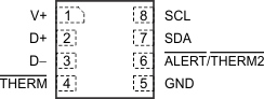
Pin Functions
| PIN | TYPE | DESCRIPTION | |
|---|---|---|---|
| NAME | NO. | ||
| ALERT/THERM2 | 6 | Digital output | Interrupt or SMBus alert output. Can be configured as a second THERM output. Open-drain; requires pullup resistor to voltage between 1.7 V and 3.6 V. |
| D– | 3 | Analog input | Negative connection to remote temperature sensor. |
| D+ | 2 | Analog input | Positive connection to remote temperature sensor. |
| GND | 5 | Ground | Supply ground connection. |
| SCL | 8 | Digital input | Serial clock line for SMBus. Input; requires pullup resistor to voltage between 1.7 V and 3.6 V if driven by open-drain output. |
| SDA | 7 | Bidirectional digital input-output | Serial data line for SMBus. Open-drain; requires pullup resistor to voltage between 1.7 V and 3.6 V. |
| THERM | 4 | Digital output | Thermal shutdown or fan-control pin. Open-drain; requires pullup resistor to voltage between 1.7 V and 3.6 V. |
| V+ | 1 | Power supply | Positive supply voltage, 1.7 V to 3.6 V. |