ZHCSEG5E October 2015 – September 2017 TMDS171
PRODUCTION DATA.
- 1 特性
- 2 应用
- 3 说明
- 4 修订历史记录
- 5 Pin Configuration and Functions
- 6 Specifications
- 7 Parameter Measurement Information
-
8 Detailed Description
- 8.1 Overview
- 8.2 Functional Block Diagram
- 8.3
Feature Description
- 8.3.1 Reset Implementation
- 8.3.2 Operation Timing
- 8.3.3 Swap and Polarity Working (Retimer Mode Only)
- 8.3.4 TMDS Inputs
- 8.3.5 TMDS Inputs Debug Tools
- 8.3.6 Receiver Equalizer
- 8.3.7 Input Signal Detect Block
- 8.3.8 Audio Return Channel
- 8.3.9 Transmitter Impedance Control
- 8.3.10 TMDS Outputs
- 8.3.11 Pre-Emphasis/De-Emphasis
- 8.4 Device Functional Modes
- 8.5
Register Maps
- 8.5.1 Local I2C Overview
- 8.5.2 CSR Bit Field Definitions, DEVICE_ID (offset: 00000000 ≈ 00000111) (reset:00h ≈ 07h)
- 8.5.3 CSR Bit Field Definitions, REV _ID (offset: 00001000) (reset: 01h)
- 8.5.4 CSR BIT Field Definitions - Misc Control (offset: 00001001) (reset: 02h)
- 8.5.5 CSR BIT Field Definitions - Misc Control (offset: 00001010) (reset: B1h)
- 8.5.6 CSR BIT Field Definitions - Misc Control (offset: 00001011) (reset: 00h)
- 8.5.7 CSR BIT Field Definitions - Misc Control (offset: 00001100) (reset: 00h)
- 8.5.8 CSR BIT Field Definitions - Equalization Control Register (offset: 00001101) (reset: 01h)
- 8.5.9 CSR BIT Field Definitions - RX Pattern Verifier Control/Status (offset: 00001110) (reset: 00h)
- 8.5.10 CSR BIT Field Definitions - RX Pattern Verifier Control/Status (offset: 00001111) (reset: 00h)
- 8.5.11 CSR BIT Field Definitions - RX Pattern Verifier Control/Status (offset: 00010000) (reset: 00h)
- 8.5.12 CSR BIT Field Definitions - RX Pattern Verifier Control/Status (offset: 00010001) (reset: 00h)
- 8.5.13 CSR BIT Field Definitions - RX Pattern Verifier Control/Status (offset: 00010010) (reset: 00h)
- 8.5.14 CSR BIT Field Definitions - RX Pattern Verifier Control/Status (offset: 00010011) (reset: 00h)
- 8.5.15 CSR BIT Field Definitions - RX Pattern Verifier Control/Status (offset: 00010100) (reset: 00h)
- 8.5.16 CSR BIT Field Definitions - RX Pattern Verifier Control/Status (offset: 00010101) (reset: 00h)
- 8.5.17 CSR BIT Field Definitions - RX Pattern Verifier Control/Status (offset: 00010110) (reset: 00h)
- 8.5.18 CSR BIT Field Definitions - RX Pattern Verifier Control/Status (offset: 00010111) (reset: 00h)
- 8.5.19 CSR BIT Field Definitions - RX Pattern Verifier Control/Status (offset: 00011000) (reset: 00h)
- 8.5.20 CSR BIT Field Definitions - RX Pattern Verifier Control/Status (offset: 00011001) (reset: 00h)
- 8.5.21 CSR BIT Field Definitions - RX Pattern Verifier Control/Status (offset: 00011010) (reset: 00h)
- 8.5.22 CSR BIT Field Definitions - RX Pattern Verifier Control/Status (offset: 00011011) (reset: 00h)
- 8.5.23 CSR BIT Field Definitions - RX Pattern Verifier Control/Status (offset: 00011100) (reset: 00h)
- 8.5.24 CSR BIT Field Definitions - RX Pattern Verifier Control/Status (offset: 00011101) (reset: 00h)
- 8.5.25 CSR BIT Field Definitions - RX Pattern Verifier Control/Status (offset: 00011110) (reset: 00h)
- 8.5.26 CSR BIT Field Definitions - RX Pattern Verifier Control/Status (offset: 00011111) (reset: 00h)
- 8.5.27 CSR BIT Field Definitions - RX Pattern Verifier Control/Status (offset: 00100000) (reset: 00h)
- 9 Application and Implementation
- 10Power Supply Recommendations
- 11Layout
- 12器件和文档支持
- 13机械、封装和可订购信息
9 Application and Implementation
NOTE
Information in the following applications sections is not part of the TI component specification, and TI does not warrant its accuracy or completeness. TI’s customers are responsible for determining suitability of components for their purposes. Customers should validate and test their design implementation to confirm system functionality.
9.1 Application Information
The TMDS171 was defined to work in many applications. This includes source applications like a Blu-Ray DVD player or AVR. The adaptive receive equalizer makes it ideal for sink applications like HDTV, monitors and projectors where cable length can be widely varied. The TMDS171 is also capable of working as an active cable to extend the cable length even further.
9.1.1 Application Chain Showing DDC Connections
The DDC circuitry inside the TMDS171 allows multiple stage operation as shown in Figure 56. The retimer devices can be connected to any of the bus segments. The number of devices that can be connected in series is limited by repeater delay/time of flight considerations for the maximum bus speed requirements.
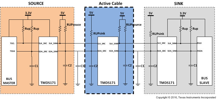 Figure 56. Typical Series Application
9.1.2 DDC Pull Up Resistors
This section is for information only and subject to change depending upon system implementation. The pull-up resistor value is determined by two requirements.
- The maximum sink current of the I2C buffer: The maximum sink current is 3 mA or slightly higher for an I2C driver supporting standard-mode I2C operation.
- The maximum transition time on the bus:

The maximum transition time, T, of an I2C bus is set by an RC time constant, where R is the pull-up resistor value, and C is the total load capacitance. The parameter, k, can be calculated from Equation 2 by solving for t, the times at which certain voltage thresholds are reached. Different input threshold combinations introduce different values of t. Table 32 summarizes the possible values of k under different threshold combinations.


Table 32. Value k upon Different Input Threshold Voltages
| Vth-\Vth+ | 0.7 VCC | 0.65 VCC | 0.6 VCC | 0.55 VCC | 0.5 VCC | 0.45 VCC | 0.4 VCC | 0.35 VCC | 0.3 VCC |
|---|---|---|---|---|---|---|---|---|---|
| 0.1 VCC | 1.0986 | 0.9445 | 0.8109 | 0.6931 | 0.5878 | 0.4925 | 0.4055 | 0.3254 | 0.2513 |
| 0.15 VCC | 1.0415 | 0.8873 | 0.7538 | 0.6360 | 0.5306 | 0.4353 | 0.3483 | 0.2683 | 0.1942 |
| 0.2 VCC | 0.9808 | 0.8267 | 0.6931 | 0.5754 | 0.4700 | 0.3747 | 0.2877 | 0.2076 | 0.1335 |
| 0.25 VCC | 0.9163 | 0.7621 | 0.6286 | 0.5108 | 0.4055 | 0.3102 | 0.2231 | 0.1431 | 0.0690 |
| 0.3 VCC | 0.8473 | 0.6931 | 0.5596 | 0.4418 | 0.3365 | 0.2412 | 0.1542 | 0.0741 |
From Equation 1, Rup(min) = 5.5 V / 3 mA = 1.83 kΩ to operate the bus under a 5-V pull-up voltage and provide less than 3 mA when the I2C device is driving the bus to a low state. If a higher sink current, for example 4 mA, is allowed, Rup(min) can be as low as 1.375 kΩ.
If DDC working at standard mode of 100 Kbps, the maximum transition time T is fixed, 1 μs, and using the k values from Table 32, the recommended maximum total resistance of the pull-up resistors on an I2C bus can be calculated for different system setups. If DDC working at fast mode of 400 Kbps, the transition time should be set at 300 ns according to I2C specification.
To support the maximum load capacitance specified in the HDMI spec, Ccable(max) = 700 pF/C(source) = 50 pF/Ci = 50 pF, R(max) can be calculated as shown in Table 33.
Table 33. Pull-Up Resistor Upon Different Threshold Voltages and 800-pF Loads
| Vth-\Vth+ | 0.7 VCC | 0.65 VCC | 0.6 VCC | 0.55 VCC | 0.5 VCC | 0.45 VCC | 0.4 VCC | 0.35 VCC | 0.3 VCC | UNIT |
|---|---|---|---|---|---|---|---|---|---|---|
| 0.1 VCC | 1.14 | 1.32 | 1.54 | 1.8 | 2.13 | 2.54 | 3.08 | 3.84 | 4.97 | KΩ |
| 0.15 VCC | 1.2 | 1.41 | 1.65 | 1.97 | 2.36 | 2.87 | 3.59 | 4.66 | 6.44 | KΩ |
| 0.2 VCC | 1.27 | 1.51 | 1.8 | 2.17 | 2.66 | 3.34 | 4.35 | 6.02 | 9.36 | KΩ |
| 0.25 VCC | 1.36 | 1.64 | 1.99 | 2.45 | 3.08 | 4.03 | 5.6 | 8.74 | 18.12 | KΩ |
| 0.3 VCC | 1.48 | 1.8 | 2.23 | 2.83 | 3.72 | 5.18 | 8.11 | 16.87 | — | KΩ |
To accommodate the 3 mA drive current specification, a narrower threshold voltage range is required to support a maximum 800 pF load capacitance for a standard-mode I2C bus.
9.2 Source Side Application
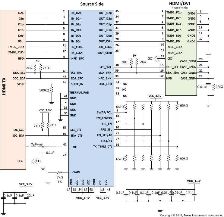 Figure 57. TMDS171 in Source Side Application
9.2.1 Design Requirements
The TMDS171 can be designed into many different applications. In all the applications there are certain requirements for the system to work properly. Two voltage rails are required in order to support lowest power consumption possible. OE pin must have a 200 nF capacitor to ground. This pin can be driven by a processor but the pin needs to change states after voltage rails have stabilized. The best way to configure the device is by using I2C but pin strapping is also provided as I2C is not available in all cases. As sources may have many different naming conventions it is necessary to confirm that the link between the source and the TMDS171 are correctly mapped. A Swap function is provide for the input pins incase signaling if reversed between source and device. Table 34 provides information on expected values in order to perform properly.
Table 34. Design Parameters
| PARAMETER | VALUE |
|---|---|
| VCC | 3.3 V |
| VDD | 1.2 V |
| Main Link Input Voltage | VID = 75 mVPP to 1.4 VPP |
| Control Pin Max Voltage for Low | 65 kΩ pulldown |
| Control Pin Voltage Range Mid | Left Not Connected/Floating |
| Control Pin Min Voltage for High | 65 kΩ pullup |
| R(VSADJ) Resistor | 7.06 kΩ 1% |
9.2.2 Detailed Design Procedure
The TMDS171 is a signal conditioning device that provides several forms of signal conditioning in order to support compliance for HDMI or DVI at a source connector. These forms of signal conditioning are accomplished using receive equalization, retiming, and output driver configurability. The transmitter will drive 2-3” of board trace and connector when compliance is required at the connector.
To design in the TMDS171 the following need to be understood for a source side application:
- Determine the loss profile between the GPU/chipset and the HDMI/DVI connector.
- Based upon this loss profile and signal swing determine optimal location for the TMDS171, in order to pass source electrical compliance. Usually within 2”-3” of the connector
- Use the typical application Figure 57 for information on control pin resistors.
- The TMDS171 has a receiver adaptive equalizer but can also be configured using EQ_SEL control pin.
- Set the VOD, Pre-emphasis, termination, and edge rate levels appropriately to support compliance by using the appropriate VSADJ resistor value and setting PRE_SEL, and TX_TERM_CTL control pins.
- The thermal pad must be connected to ground.
- See Figure 57 for recommended decouple capacitors from VCC and VDD pins to Ground
9.2.3 Application Curves
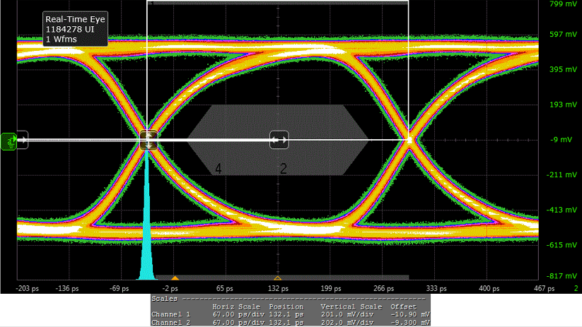 Figure 58. 1080p Compliance Eye
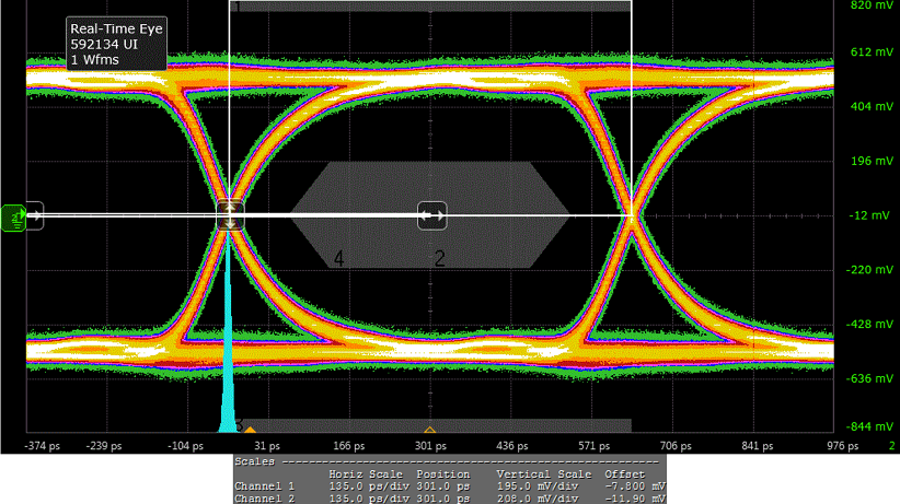 Figure 59. 4k2k30 Compliance Eye
9.2.4 Sink Side Application
For a sink side application HPD needs consideration. The TMDS171 drives the HPD signal to 3.3V which meetings requirements but if 5 V HPD signaling is required the two circuits shown in Figure 60 are required. As sources are not consistent in implementing all aspects of the DDC link it is recommended to configure the TMDS171 as per Figure 60. Another consideration in relationship to how HPD is implemented is the architecture and behavior of the HDMI RX/Scalar.
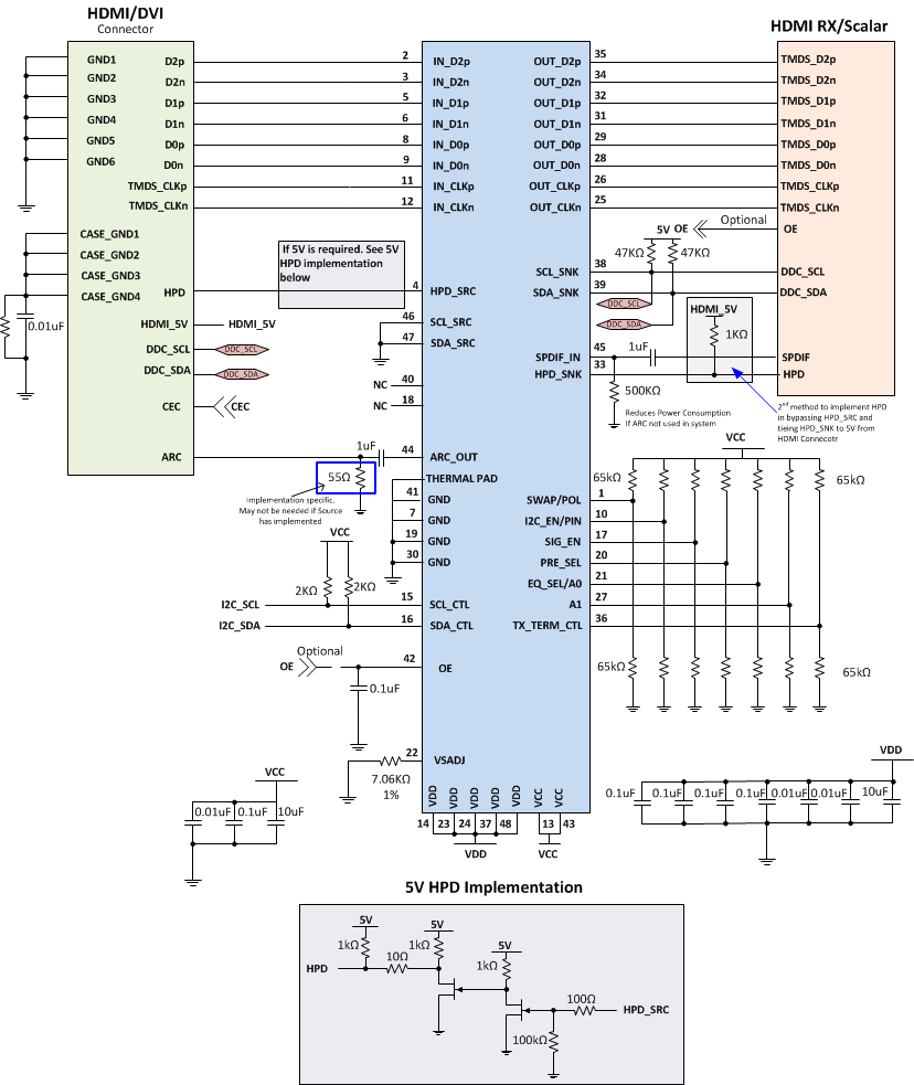 Figure 60. TMDS171 in Sink Side Application, 5 V HPD Implementation
9.2.4.1 Design Requirements
See Table 35 for the Sink Side design example parameters.
Table 35. Design Parameters
| PARAMETER | VALUE |
|---|---|
| VCC | 3.3 V |
| VDD | 1.2 V |
| Main Link Input Voltage | VID = 75 mVPP to 1.4 VPP |
| Control Pin Max Voltage for Low | 65 kΩ pulldown |
| Control Pin Voltage Range Mid | Left Not Connected/Floating |
| Control Pin Min Voltage for High | 65 kΩ pullup |
| R(VSADJ) Resistor | 7.06 kΩ 1% |
9.2.4.2 Detailed Design Procedure
To design in the TMDS171 the following need to be understood for a source side application.
- Determine the loss profile between the RX/chipset and the HDMI/DVI connector.
- Based upon this loss profile and signal swing determine optimal location for the TMDS171, in order to pass sink electrical compliance.
- Use the typical application Figure 56 for information on control pin resistors.
- The TMDS171 has a receiver adaptive equalizer but can also be configured using EQ_SEL control pin.
- Set the VOD, Pre-emphasis, termination, and edge rate levels appropriately to support link between TMDS171 and HDMI RX/Chipset by using the appropriate VSADJ resistor value and setting PRE_SEL and TX_TERM_CTL control pins.
- The thermal pad must be connected to ground.
- See Figure 60 for recommended decouple caps from VCC and VDD pins to Ground.
9.3 System Examples
Another way to configure sink application is to configure the sink as per Figure 61. This is done as not all sources are supporting clock stretching as per standard.
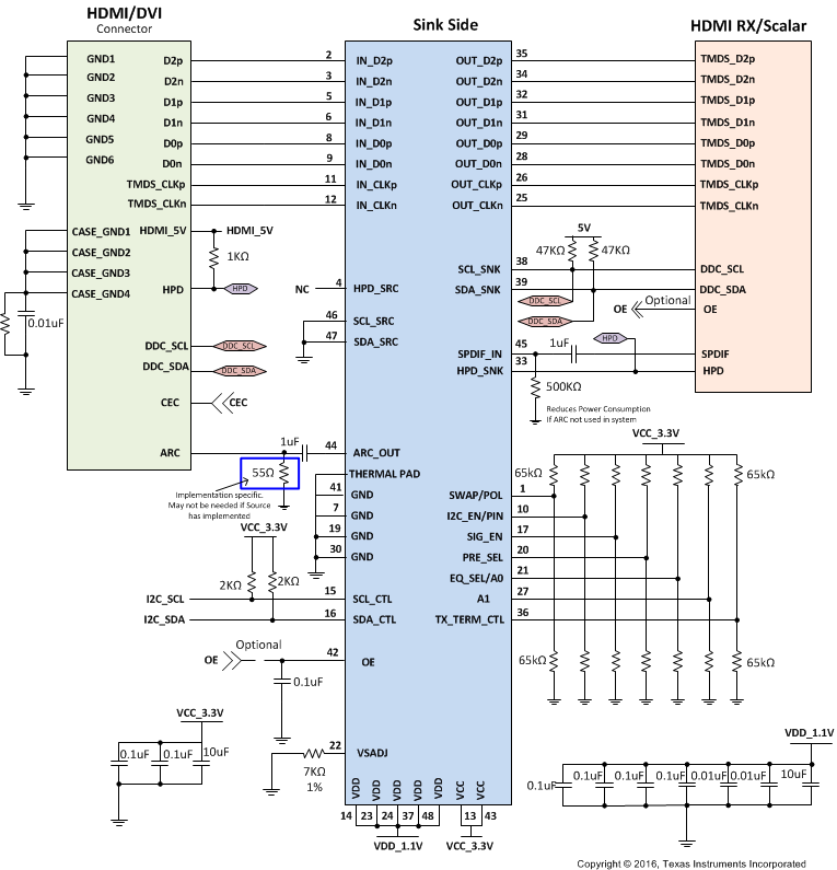 Figure 61. TMDS171 in Sink Side Application