ZHCSL40N November 2004 – June 2024 TLVH431 , TLVH431A , TLVH431B , TLVH432 , TLVH432A , TLVH432B
PRODUCTION DATA
- 1
- 1 特性
- 2 应用
- 3 说明
- 4 Pin Configuration and Functions
- 5 Specifications
- 6 Parameter Measurement Information
- 7 Detailed Description
- 8 Applications and Implementation
- 9 Device and Documentation Support
- 10Revision History
- 11Mechanical, Packaging, and Orderable Information
封装选项
机械数据 (封装 | 引脚)
散热焊盘机械数据 (封装 | 引脚)
- PK|3
订购信息
5.7 TLVH43xB Electrical Characteristics
at 25°C free-air temperature (unless otherwise noted)
| PARAMETER | TEST CONDITIONS | TLVH431B TLVH432B | UNIT | |||||
|---|---|---|---|---|---|---|---|---|
| MIN | TYP | MAX | ||||||
| VREF | Reference voltage | VKA = VREF, IK = 10mA | TA = 25°C | 1.234 | 1.24 | 1.246 | V | |
| TA = full range, See Figure 6-1(1) | TLVH431BC | 1.227 | 1.253 | |||||
| TLVH431BI | 1.224 | 1.259 | ||||||
| TLVH431BQ | 1.221 | 1.265 | ||||||
| VREF(dev) | VREF deviation over full temperature range(2) | VKA = VREF, IK = 10mA, See Figure 6-1(1) | TLVH431BC | 4 | 12 | mV | ||
| TLVH431BI | 6 | 20 | ||||||
| TLVH431BQ | 11 | 31 | ||||||
 | Ratio of VREF change to cathode voltage change | IK = 10mA, VK = VREF to 18V, See Figure 6-2 | –1.5 | –2.7 | mV/V | |||
| Iref | Reference terminal current | IK = 10mA, R1 = 10kΩ, R2 = open, See Figure 6-2 | 0.1 | 0.5 | μA | |||
| Iref(dev) | Iref deviation over full temperature range(2) | IK = 10mA, R1 = 10kΩ, R2 = open, See Figure 6-2(1) | TLVH431BC | 0.05 | 0.3 | μA | ||
| TLVH431BI | 0.1 | 0.4 | ||||||
| TLVH431BQ | 0.15 | 0.5 | ||||||
| IK(min) | Minimum cathode current for regulation | VKA = VREF, See Figure 6-1 | 60 | 100 | μA | |||
| IK(off) | Off-state cathode current | VREF = 0, VKA = 18V, See Figure 6-3 | 0.02 | 0.1 | μA | |||
| |zKA| | Dynamic impedance(3) | VKA = VREF, f ≤ 1kHz, IK = 0.1mA to 70mA, See Figure 6-1 | 0.25 | 0.4 | Ω | |||
(1) Full temperature ranges are –40°C to +125°C for TLVH431Q, –40°C to +85°C for TLVH431I, and 0°C to 70°C for TLVH431C.
(2) The deviation parameters VREF(dev) and Iref(dev) are defined as the differences between the maximum and minimum values obtained over the rated temperature range. The average full-range temperature coefficient of the reference input voltage, αVREF, is defined as:
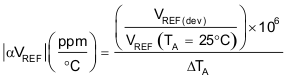
where ΔTA is the rated operating free-air temperature range of the device.
αVREF can be positive or negative, depending on whether minimum VREF or maximum VREF, respectively, occurs at the lower temperature.
where ΔTA is the rated operating free-air temperature range of the device.
αVREF can be positive or negative, depending on whether minimum VREF or maximum VREF, respectively, occurs at the lower temperature.
(3) The dynamic impedance is defined as:

When the device is operating with two external resistors (see Figure 6-2), the total dynamic impedance of the circuit is defined as:

When the device is operating with two external resistors (see Figure 6-2), the total dynamic impedance of the circuit is defined as: