ZHCSGW3A June 2017 – October 2017 TLV760
PRODUCTION DATA.
7 Detailed Description
7.1 Overview
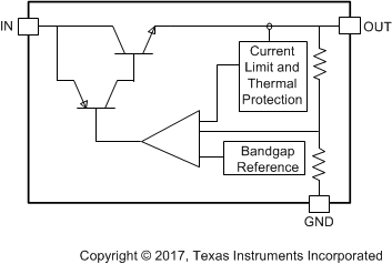
The TLV760 is an integrated linear-voltage regulator with inputs that can be as high as 30 V. The TLV760 features quasi LDO architecture, which allows the usage of low ESR capacitors at the output. A ceramic capacitor with a capacitance value greater than or equal to 0.1 µF is adequate to keep the linear regulator in stable operation. The device has a rugged active junction thermal protection mechanism.
7.2 Functional Block Diagram

7.3 Feature Description
7.3.1 Thermal Protection
The TLV760 contains an active thermal protection mechanism, which limits the junction temperature to 150°C. This protection comes into action when the thermal junction temperature of the device tries to exceed 150°C. The output current of the device is limited or folded back to maintain the junction temperature.
The thermal protection follows Equation 1

where
- PD = (VIN – VOUT )IOUT
- TJ is the junction temperature
- RθJA is the junction-to-ambient thermal resistance
When a high drop out condition occurs resulting in higher power dissipation across the device the output current is limited to maintain a constant junction temperature of 150°C. This rugged feature protects the device from higher power dissipation applications as well as the short to ground at the output.
This internal protection circuitry of TLV760 is intended to protect the devices against thermal overload conditions. The circuitry is not intended to replace proper heat sinking. Continuously running the TLV760 into thermal protection degrades device reliability.
For reliable operation, limit junction temperature to a maximum of 125°C. To estimate the thermal margin in a given layout, increase the ambient temperature until the thermal protection is triggered using worst case load and highest input voltage conditions.
7.3.2 Dropout Voltage
The TLV760 is a bipolar device with quasi LDO architecture. Being a bipolar device the dropout voltage of the device does not change significantly with output load current. The device has a maximum dropout across temperature of 1.2 V at 100-mA load current, which is a significant improvement over the traditional LM78Lxx devices.
7.4 Device Functional Modes
7.4.1 Normal Operation
The TLV760 operates with an input up to 30 V. Its tiny SOT-23 package and quasi-LDO architecture makes it suitable for providing a very tiny 100-mA bias supply. The device regulates to the nominal output voltage when all of the following conditions are met.
- The input voltage is greater than the nominal output voltage plus the dropout voltage (VOUT(NOM) + VDO).
- The output current is less than or equal to 100 mA.
- The device junction temperature is less than the thermal protection temperature of 150°C.