ZHCSGW3A June 2017 – October 2017 TLV760
PRODUCTION DATA.
6 Specifications
6.1 Absolute Maximum Ratings(1)
| MIN | MAX | UNIT | |
|---|---|---|---|
| Input voltage (IN to GND) | –0.3 | 35 | V |
| Output Voltage (OUT) | VIN + 0.3 | V | |
| Output Current | Internally limited(2) | mA | |
| Junction temperature | –40 | 150 | °C |
| Storage temperature, Tstg | −65 | 150 | °C |
(1) Stresses beyond those listed under Absolute Maximum Ratings may cause permanent damage to the device. These are stress ratings only, which do not imply functional operation of the device at these or any other conditions beyond those indicated under Recommended Operating Conditions. Exposure to absolute-maximum-rated conditions for extended periods may affect device reliability.
(2) See Recommended Operating Conditions section for more details.
6.2 ESD Ratings
| VALUE | UNIT | |||
|---|---|---|---|---|
| V(ESD) | Electrostatic discharge | Human-body model (HBM), per ANSI/ESDA/JEDEC JS-001(1) | ±2000 | V |
| Charged-device model (CDM), per JEDEC specification JESD22-C101(2) | ±500 | |||
(1) JEDEC document JEP155 states that 500-V HBM allows safe manufacturing with a standard ESD control process.
(2) JEDEC document JEP157 states that 250-V CDM allows safe manufacturing with a standard ESD control process.
6.3 Recommended Operating Conditions
over operating free-air temperature range (unless otherwise noted)| MIN | MAX | UNIT | |
|---|---|---|---|
| Maximum input voltage (IN to GND) | 30 | V | |
| Output current (IOUT) | 100 | mA | |
| Input and output capacitor (COUT) | 0.1 | µF | |
| Junction temperature, TJ | –40 | 125 | °C |
6.4 Thermal Information
| THERMAL METRIC(1) | TLV760 | UNIT | |
|---|---|---|---|
| DBZ (SOT-23) | |||
| 3 PINS | |||
| RθJA | Junction-to-ambient thermal resistance | 275.2 | °C/W |
| RθJC(top) | Junction-to-case (top) thermal resistance | 92.8 | °C/W |
| RθJB | Junction-to-board thermal resistance | 56.8 | °C/W |
| ψJT | Junction-to-top characterization parameter | 2.9 | °C/W |
| ψJB | Junction-to-board characterization parameter | 55.6 | °C/W |
(1) For more information about traditional and new thermal metrics, see the Semiconductor and IC Package Thermal Metrics application report.
6.5 Electrical Characteristics
Typical and other limits apply for TA = TJ = 25°C, VOUT(NOM) = 3.3 V, 5 V, 12 V, and 15 V, unless otherwise specified.| PARAMETER | TEST CONDITIONS | MIN | TYP | MAX | UNIT | ||
|---|---|---|---|---|---|---|---|
| VOUT | Output voltage accuracy | VIN = VOUT(NOM)+ 1.5 V, 1 mA ≤ IOUT ≤ 100 mA |
–4% | 4% | V | ||
| VIN = VOUT(NOM) + 1.5 V, 1 mA ≤ IOUT ≤ 100 mA, −40°C ≤ TJ ≤ 125°C |
–5% | 5% | |||||
| ΔV(ΔVIN) | Line regulation | VOUT(NOM) + 1.5 V ≤ VIN ≤ 30 V IOUT = 1 mA , −40°C ≤ TJ ≤ 125°C |
VOUT(NOM) = 3.3 V, 5 V | 10 | 30 | mV | |
| VOUT(NOM) = 12 V, 15 V | 14 | 45 | |||||
| ΔV(ΔIOUT) | Load regulation | VIN =VOUT(NOM) + 1.5 V , 10 mA ≤ IOUT ≤ 100 mA, −40°C ≤ TJ ≤ 125°C |
VOUT(NOM) = 3.3 V, 5 V | 20 | 45 | mV | |
| VOUT(NOM) = 12 V, 15 V | 45 | 80 | |||||
| IGND | Ground pin current | VOUT(NOM) + 1.5 V ≤ VIN ≤ 30 V, no load, −40°C ≤ TJ ≤ 125°C |
2 | 5 | mA | ||
| VDO | Dropout voltage | IOUT = 10 mA | 0.7 | 0.9 | V | ||
| IOUT = 10 mA , −40°C ≤ TJ ≤ 125°C | 1 | ||||||
| IOUT = 100 mA | 0.9 | 1.1 | |||||
| IOUT = 100 mA, −40°C ≤ TJ ≤ 125°C | 1.2 | ||||||
| TSD | Thermal shutdown temperature | 150 | °C | ||||
6.6 Typical Characteristics
Unless indicated otherwise, VIN = VNOM + 1.5 V, CIN = 0.1 µF, COUT = 0.1 µF, and TA = 25°C.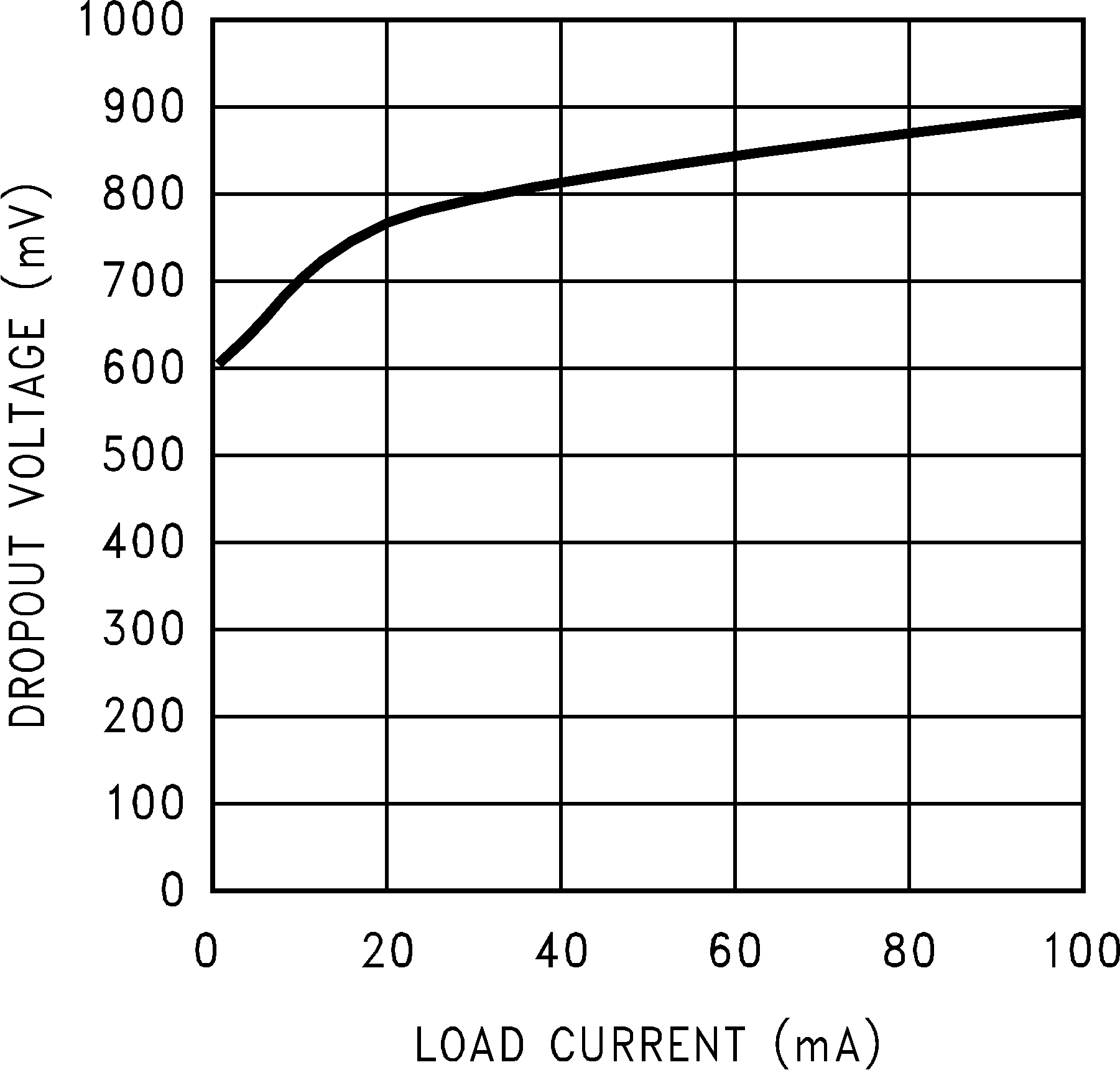 Figure 1. Dropout Voltage vs Load Current
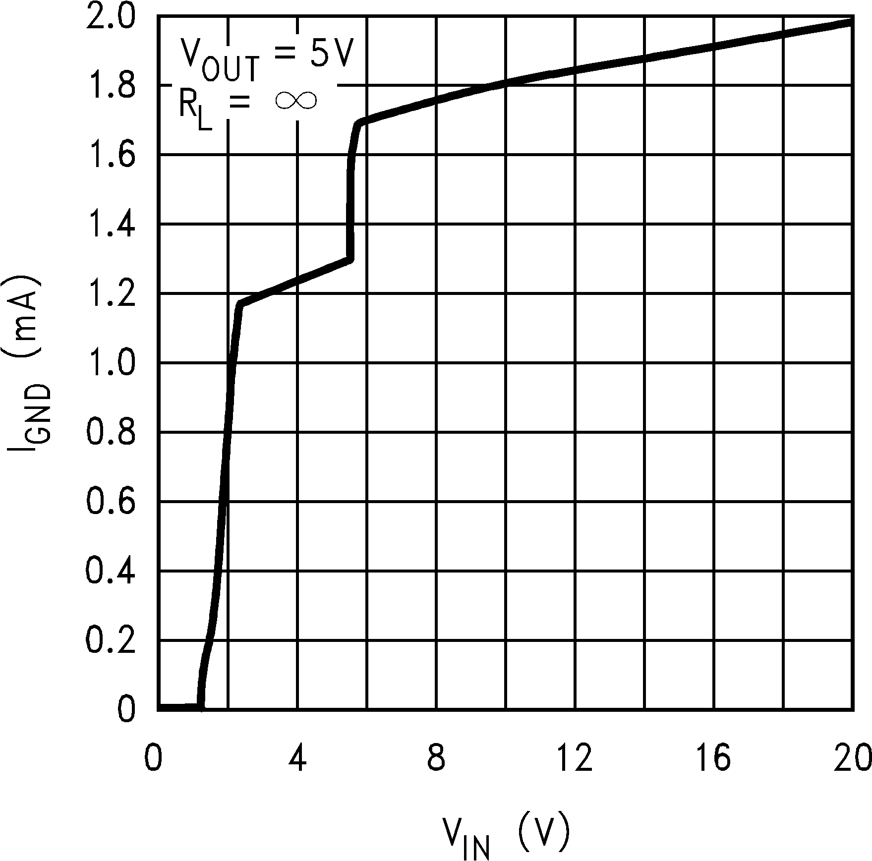 Figure 3. Ground Pin Current vs Input Voltage
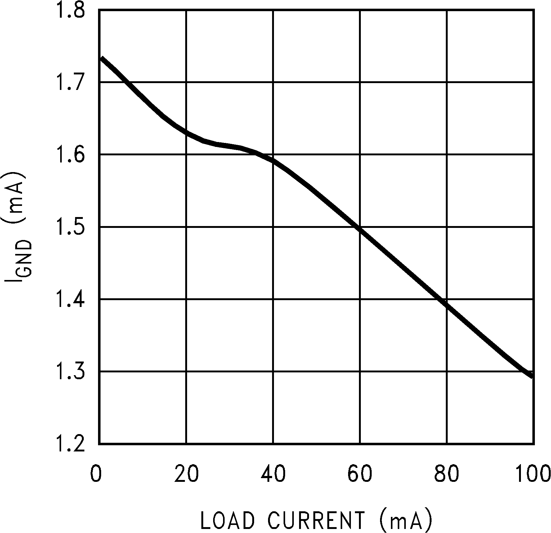 Figure 5. Ground Pin Current vs Load Current
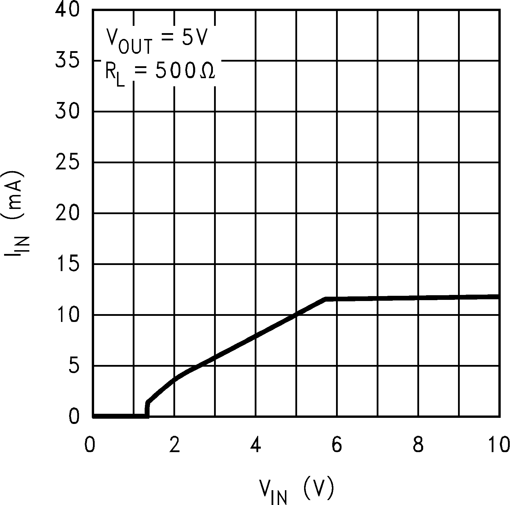 Figure 7. Input Current vs Input Voltage
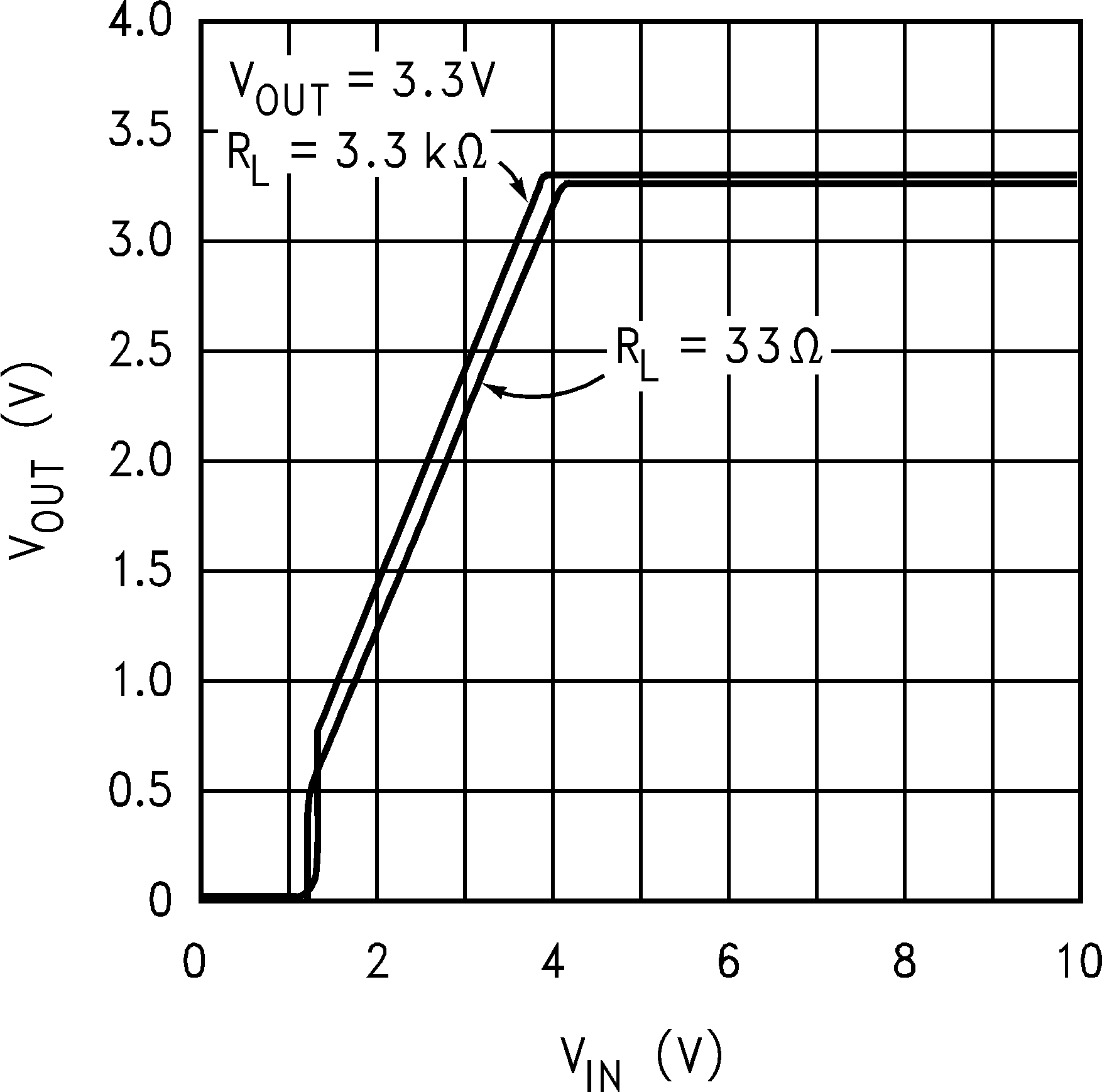 Figure 9. Output Voltage vs Input Voltage
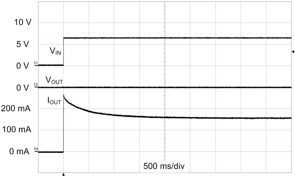
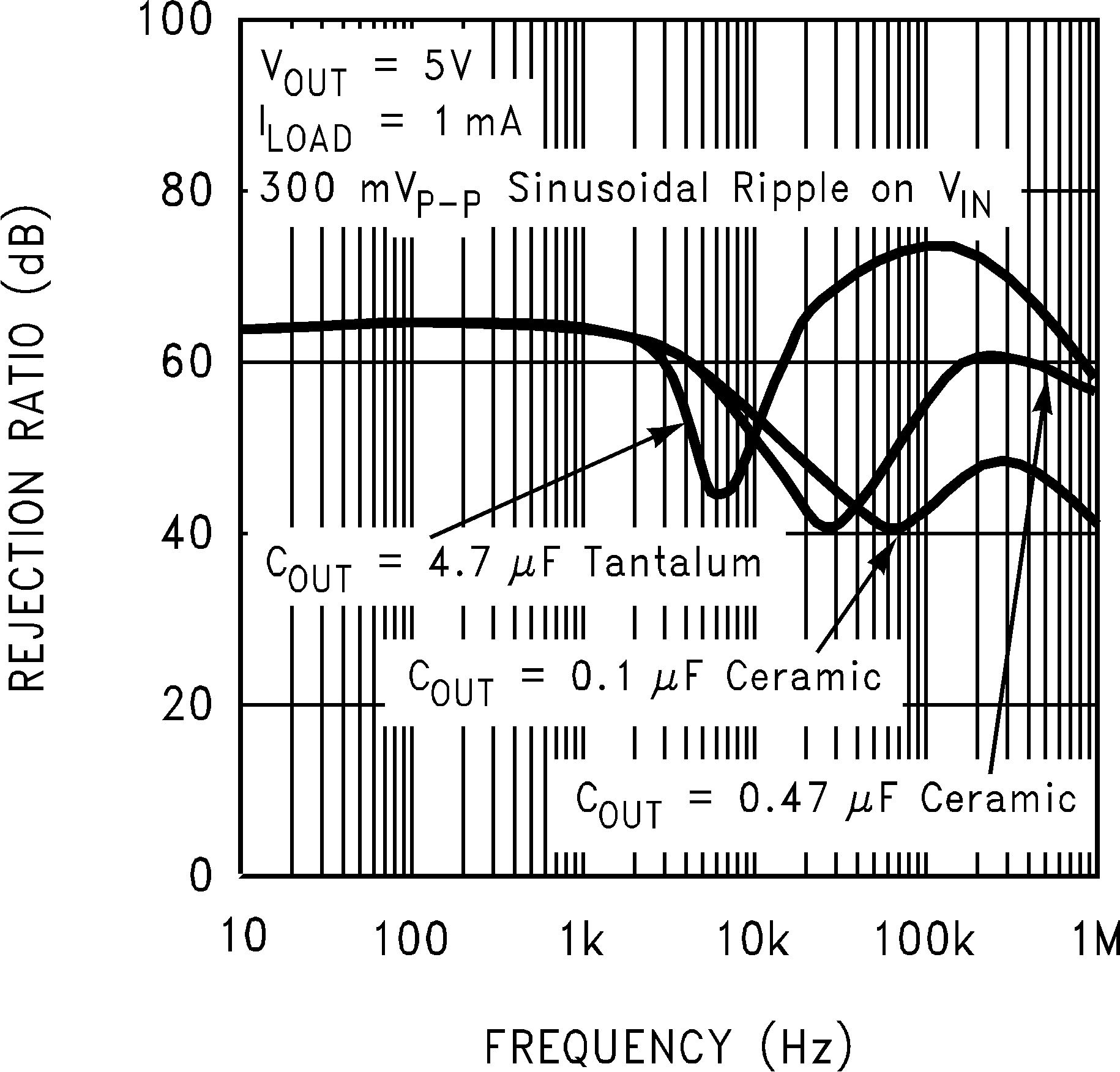 Figure 13. Power Supply Rejection Ratio
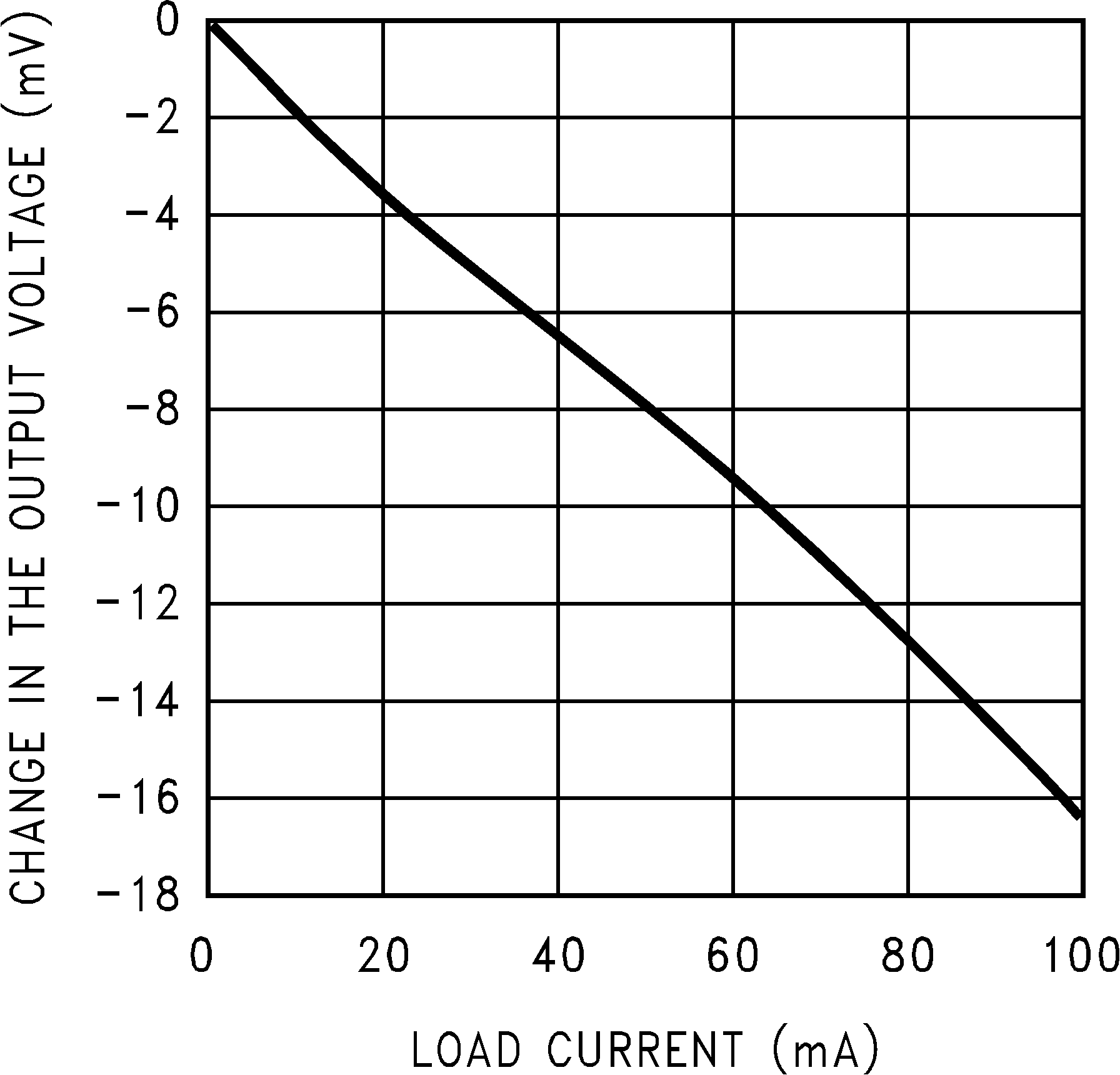 Figure 15. DC Load Regulation
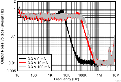
| CIN = 1 µF | COUT = 0.1 µF | VOUT = 3.3 V | ||
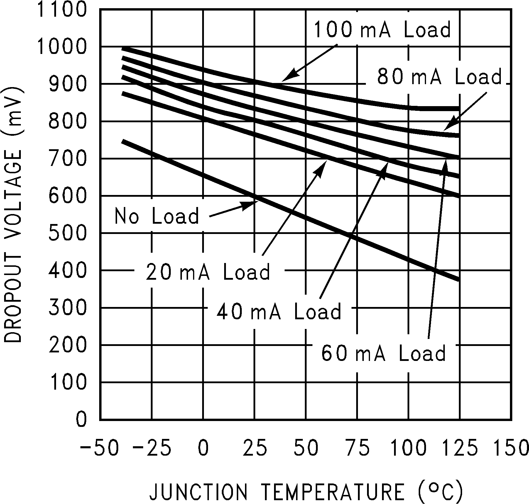 Figure 2. Dropout Voltage vs Junction Temperature
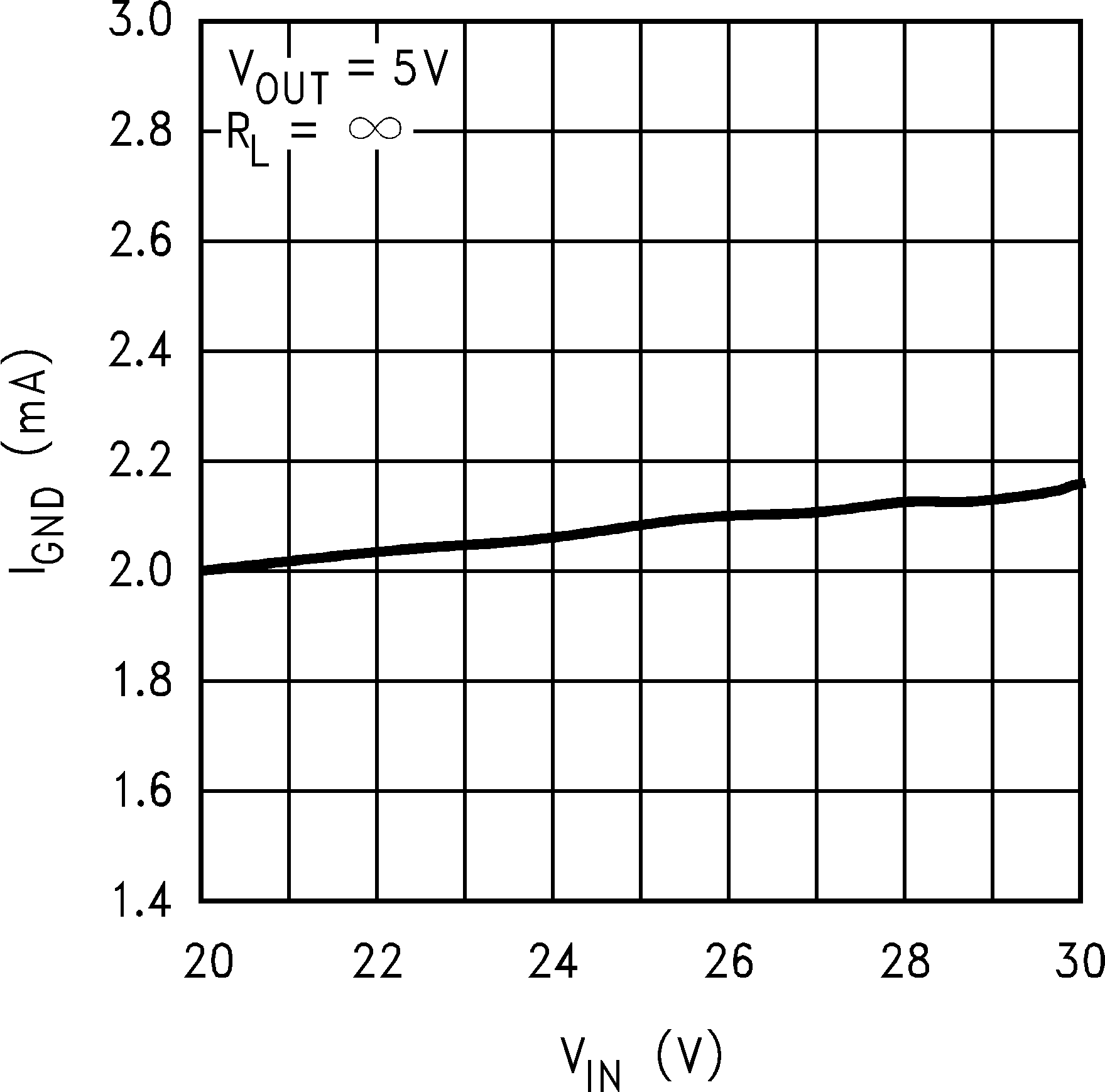 Figure 4. Ground Pin Current vs Input Voltage
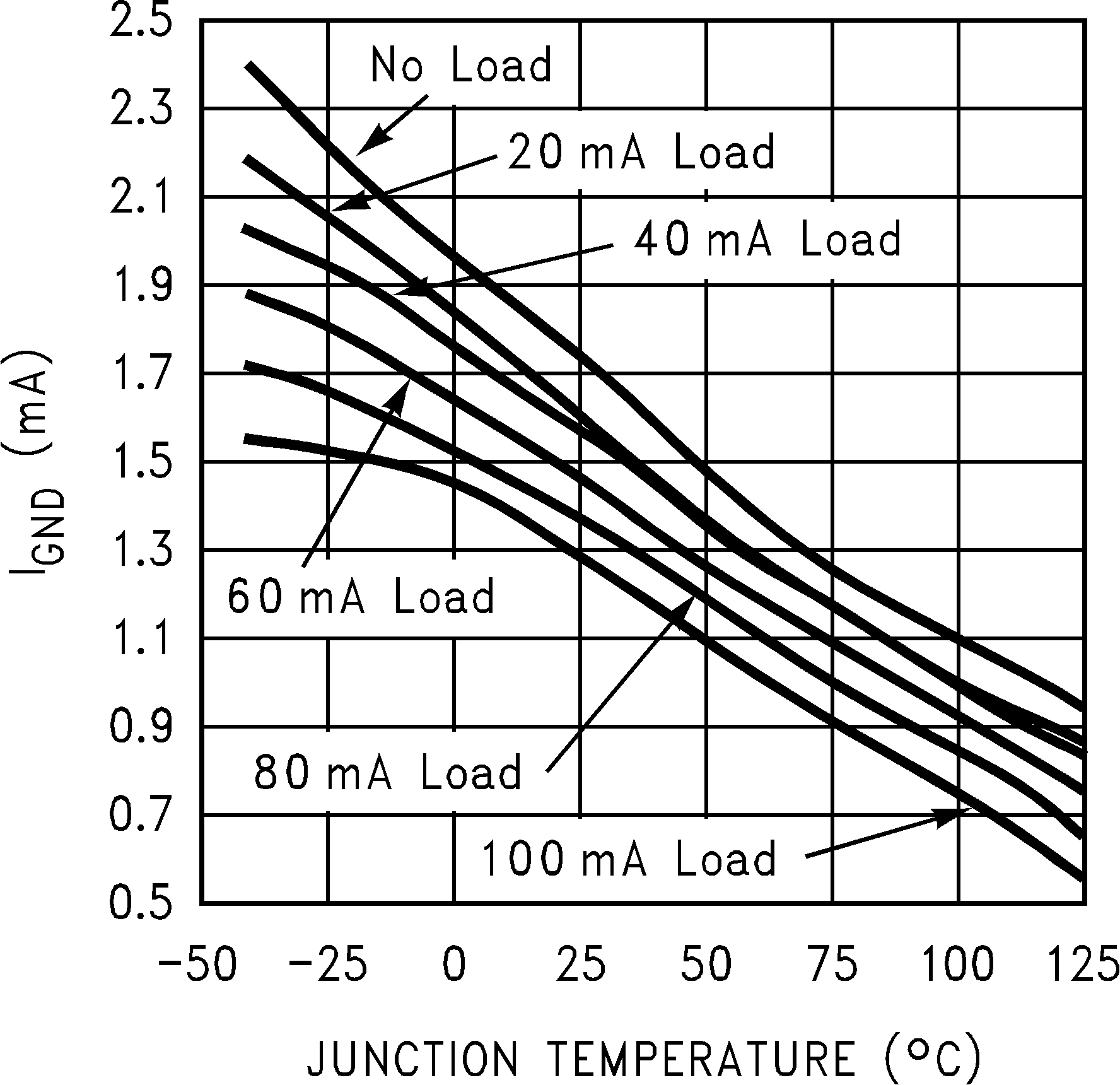 Figure 6. Ground Pin Current vs Junction Temperature
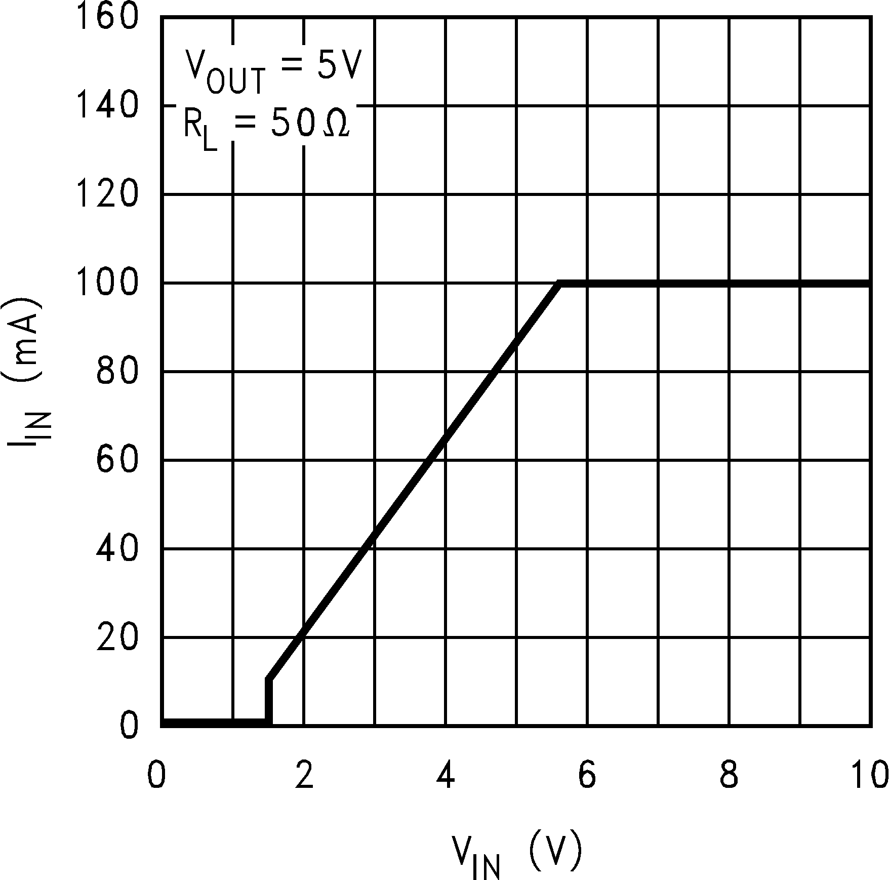 Figure 8. Input Current vs Input Voltage
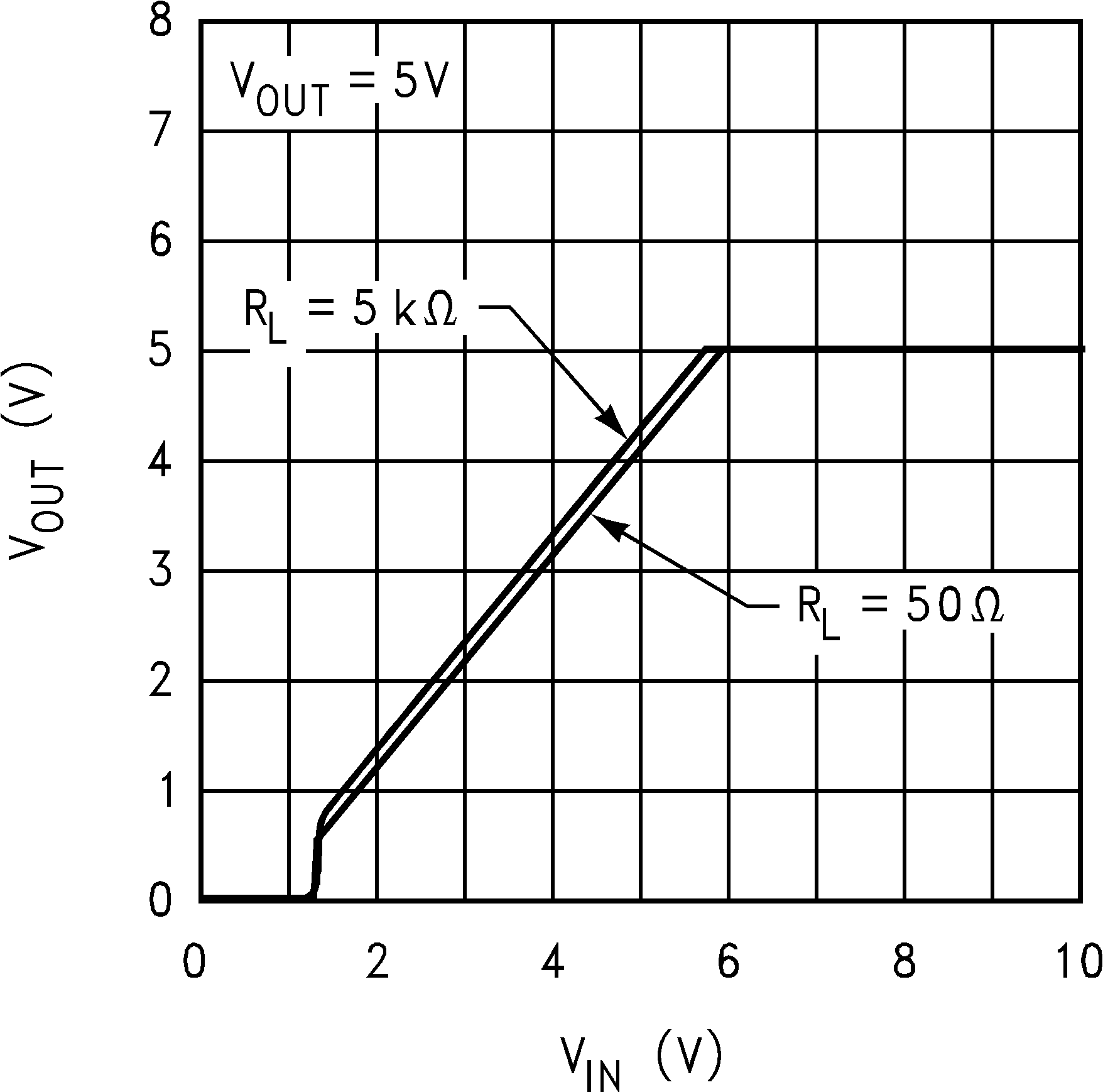 Figure 10. Output Voltage vs Input Voltage
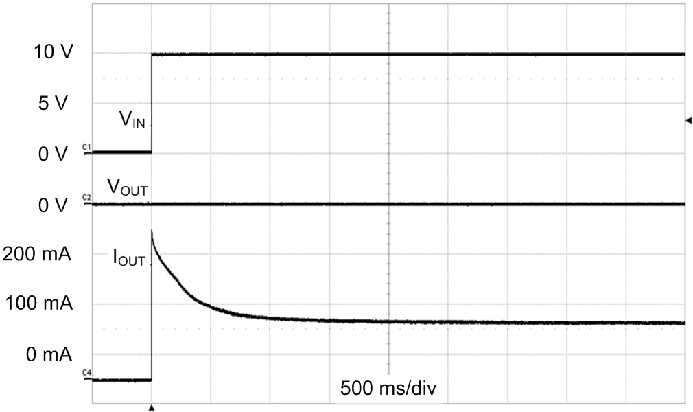
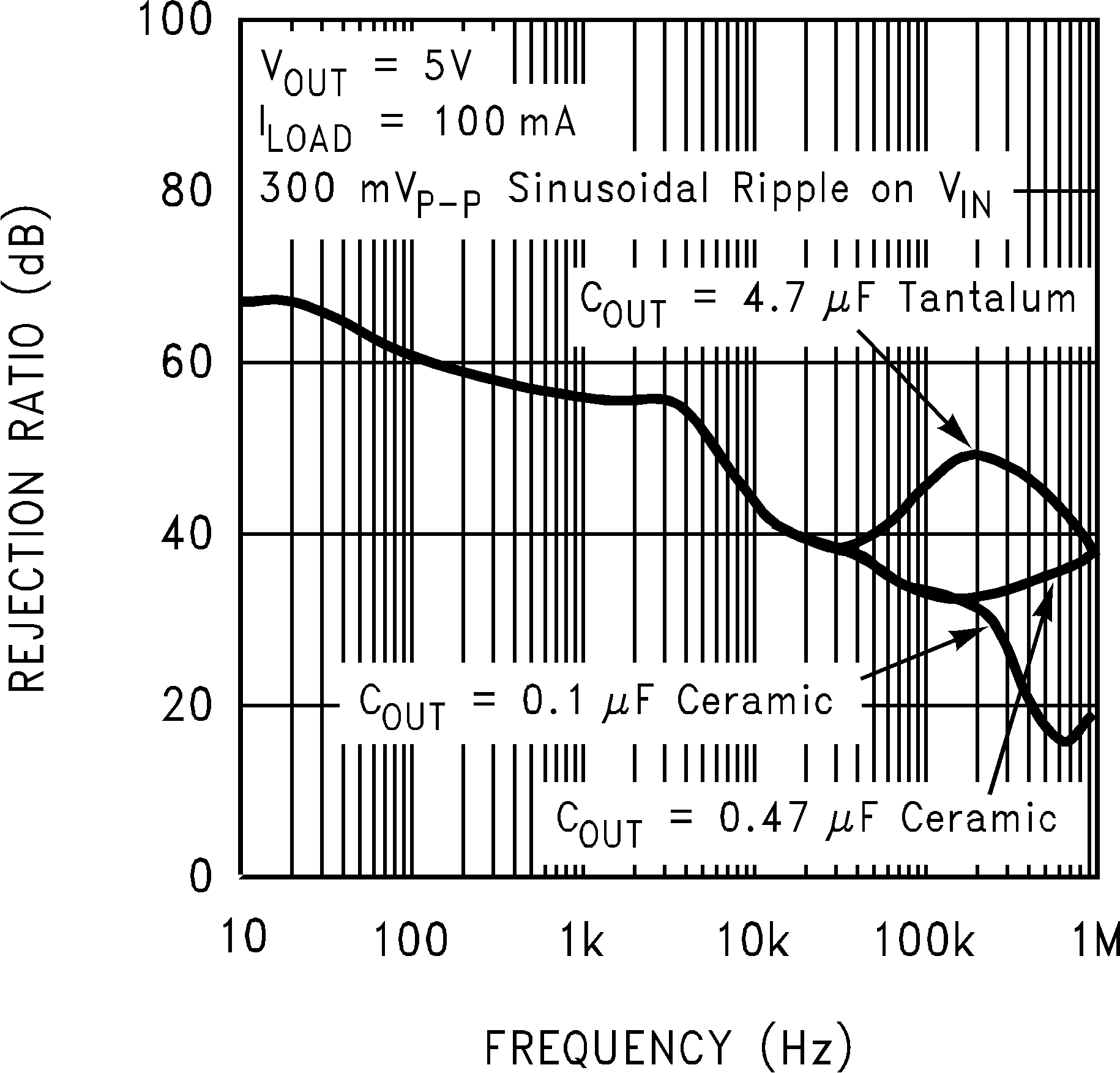 Figure 14. Power Supply Rejection Ratio
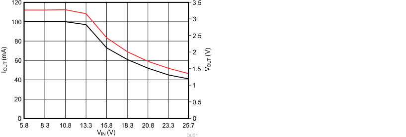
| VOUT(Red) = 3.3 V | IOUT(Black) = 100 mA | |