ZHCSF26 May   2016 TLV522

PRODUCTION DATA.  

  1. 特性
  2. 应用
  3. 说明
  4. 修订历史记录
  5. Pin Configuration and Functions
  6. Specifications
    1. 6.1 Absolute Maximum Ratings
    2. 6.2 ESD Ratings
    3. 6.3 Recommended Operating Ratings
    4. 6.4 Thermal Information
    5. 6.5 Electrical Characteristics
    6. 6.6 Typical Characteristics
  7. Detailed Description
    1. 7.1 Overview
    2. 7.2 Functional Block Diagram
    3. 7.3 Feature Description
    4. 7.4 Device Functional Modes
      1. 7.4.1 Rail-To-Rail Input
      2. 7.4.2 Supply Current Changes Over Common Mode
      3. 7.4.3 Design Optimization With Rail-To-Rail Input
      4. 7.4.4 Design Optimization for Nanopower Operation
      5. 7.4.5 Common-Mode Rejection
      6. 7.4.6 Output Stage
      7. 7.4.7 Driving Capacitive Load
  8. Application and Implementation
    1. 8.1 Application Information
    2. 8.2 Typical Application: 60 Hz Twin "T" Notch Filter
      1. 8.2.1 Design Requirements
      2. 8.2.2 Detailed Design Procedure
      3. 8.2.3 Application Curve
    3. 8.3 Do's and Don'ts
  9. Power Supply Recommendations
  10. 10Layout
    1. 10.1 Layout Guidelines
    2. 10.2 Layout Example
  11. 11器件和文档支持
    1. 11.1 器件支持
      1. 11.1.1 开发支持
    2. 11.2 文档支持
      1. 11.2.1 相关文档 
    3. 11.3 社区资源
    4. 11.4 商标
    5. 11.5 静电放电警告
    6. 11.6 Glossary
  12. 12机械、封装和可订购信息

封装选项

机械数据 (封装 | 引脚)
散热焊盘机械数据 (封装 | 引脚)
订购信息

5 Pin Configuration and Functions

8-Pin VSSOP
DGK Package
Top View
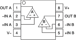
TLV522 po_2333_so_msop_bos351.gif

Pin Functions

PIN I/O DESCRIPTION
PIN NAME
1 OUT A O Channel A Output
2 –IN A I Channel A Inverting Input
3 +IN A I Channel A Non-Inverting Input
4 V– P Negative (lowest) power supply
5 +IN B I Channel B Non-Inverting Input
6 –IN B I Channel B Inverting Input
7 OUT B O Channel B Output
8 V+ P Positive (highest) power supply