ZHCSR71 October   2020 TLV4062-Q1 , TLV4082-Q1

PRODUCTION DATA  

  1. 特性
  2. 应用
  3. 说明
  4. Revision History
  5. Pin Configuration and Functions
  6. Specifications
    1. 6.1 Absolute Maximum Ratings
    2. 6.2 ESD Ratings
    3. 6.3 Recommended Operating Conditions
    4. 6.4 Thermal Information
    5. 6.5 Electrical Characteristics
    6. 6.6 Timing Requirements
    7. 6.7 Timing Diagrams
    8. 6.8 Typical Characteristics
  7. Detailed Description
    1. 7.1 Overview
    2. 7.2 Functional Block Diagrams
    3. 7.3 Feature Description
    4. 7.4 Device Functional Modes
      1. 7.4.1 Inputs (IN1, IN2)
      2. 7.4.2 Outputs (OUT1, OUT2)
      3. 7.4.3 Switching Threshold and Hysteresis
  8. Application and Implementation
    1. 8.1 Application Information
      1. 8.1.1 Threshold Overdrive
    2. 8.2 Typical Applications
      1. 8.2.1 Monitoring Two Separate Rails
        1. 8.2.1.1 Design Requirements
        2. 8.2.1.2 Detailed Design Procedure
        3. 8.2.1.3 Application Curve
      2. 8.2.2 Early Warning Detection
        1. 8.2.2.1 Design Requirements
        2. 8.2.2.2 Detailed Design Procedure
        3. 8.2.2.3 Application Curve
      3. 8.2.3 Additional Application Information
        1. 8.2.3.1 Pull-Up Resistor Selection
        2. 8.2.3.2 INx Capacitor
  9. Power Supply Recommendations
  10. 10Layout
    1. 10.1 Layout Guidelines
    2. 10.2 Layout Example
  11. 11Device and Documentation Support
    1. 11.1 Documentation Support
      1. 11.1.1 Related Documentation
    2. 11.2 Receiving Notification of Documentation Updates
    3. 11.3 支持资源
    4. 11.4 Trademarks
    5. 11.5 静电放电警告
    6. 11.6 术语表
      1.      Mechanical, Packaging, and Orderable Information

封装选项

机械数据 (封装 | 引脚)
散热焊盘机械数据 (封装 | 引脚)
订购信息

Typical Characteristics

at TJ = 25°C with a 0.1-µF capacitor close to V+ (unless otherwise noted)
GUID-825F1D81-E967-4A2C-A4D7-12DC31A3D2DE-low.gif
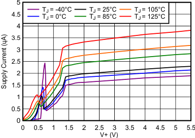
IN1 = IN2 = 1.5 V
Figure 6-2 Supply Current vs Supply Voltage
GUID-F55DD948-BB80-44FB-9933-7160B2A37278-low.gif
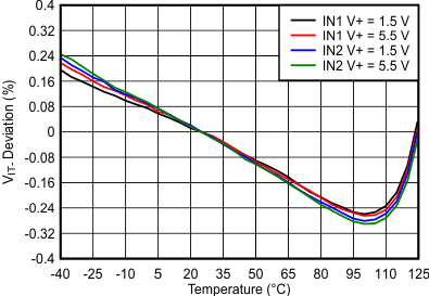
Figure 6-4 INx Threshold (VIT–) Deviation vs Temperature
GUID-E8E76B09-A896-496A-BF54-AF04242E77DD-low.gif
V+ = 5.5 V
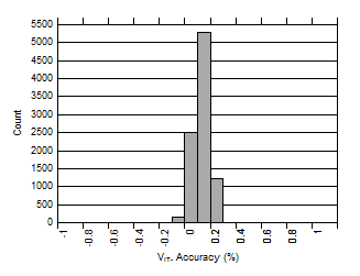
Figure 6-6 INx Threshold (VIT–)
GUID-A26C40A6-82F5-463C-B8E4-5D9735C2F53D-low.gif
Figure 6-8 Output Voltage Low vs Output Current (V+ = 3.3 V)
GUID-15F8121F-30A7-4384-9D3C-502C6A22C06F-low.gif
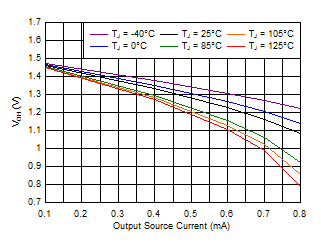
Figure 6-10 Output Voltage High vs Output Current (V+ = 1.5 V)
GUID-42086255-9DE7-43B1-AE13-7F79356D1491-low.gif
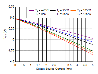
Figure 6-12 Output Voltage High vs Output Current (V+ = 5.5 V)
GUID-9A54B6F5-07C5-4B77-BD8A-D58A3230A3C6-low.gif
IN1 = IN2 = 1.3 V to 0 V
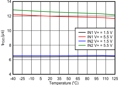
Figure 6-14 Propagation Delay from INx Low to Output Low
GUID-10EED823-6631-4541-BC34-132D415E9A9E-low.gif
High-to-low transition occurs above the curve
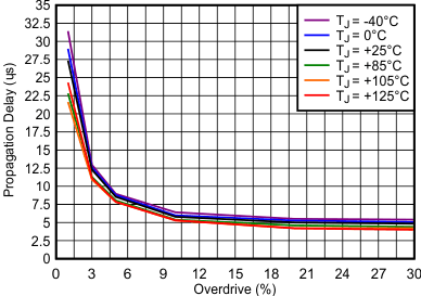
Figure 6-16 Propagation Delay vs Overdrive (V+ = 1.5 V)
GUID-72E7FC92-2B14-43D9-A4F8-F919C3A5556C-low.gif
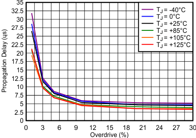
Low-to-high transition occurs above the curve
Figure 6-18 Propagation Delay vs Overdrive (V+ = 1.5 V)
GUID-8471532D-D94A-4845-B91B-62FDA59E4313-low.gif
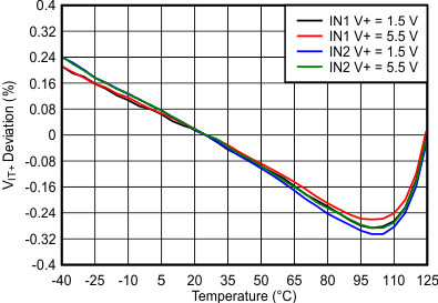
Figure 6-3 INx Threshold (VIT+) Deviation vs Temperature
GUID-20F17969-2859-4E76-A6EE-0123E13341C2-low.gif
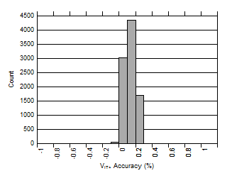
V+ = 5.5 V
Figure 6-5 INx Threshold (VIT+)
GUID-391788CF-2691-4D35-98FF-B9868331041C-low.gif
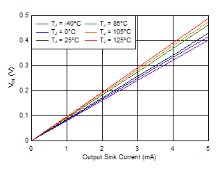
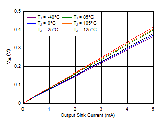
Figure 6-7 Output Voltage Low vs Output Current (V+ = 1.5 V)
GUID-4F496BFF-96F9-4B55-94AA-3047A79A7A0A-low.gif
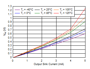
Figure 6-9 Output Voltage Low vs Output Current (V+ = 5.5 V)
GUID-1D4D63ED-1AB4-48EB-AAFA-B2061FFB0362-low.gif
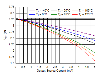
Figure 6-11 Output Voltage High vs Output Current (V+ = 3.3 V)
GUID-355E6AF5-2FD4-4279-8037-A5006C436A81-low.gif
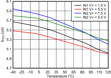
IN1 = IN2 = 0 V to 1.3 V
Figure 6-13 Propagation Delay from INx High to Output High
GUID-EC1DE091-76AB-4AC2-9F9F-65DDA3B5ACE4-low.gif
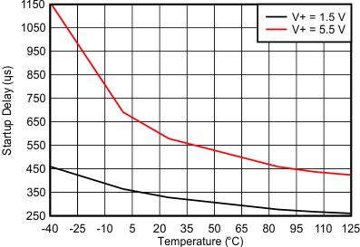
Figure 6-15 Startup Delay
GUID-B01DC609-925F-409E-8157-97DDFCB3BF8D-low.gif
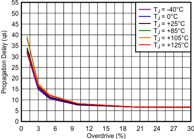
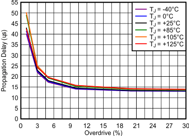
High-to-low transition occurs above the curve
Figure 6-17 Propagation Delay vs Overdrive (V+ = 5.5 V)
GUID-0055DDE5-567F-42D1-BE34-E9ABB928A9D9-low.gif
Low-to-high transition occurs above the curve
Figure 6-19 Propagation Delay vs Overdrive (V+ = 5.5 V)