SBVS404A April   2020  – June 2020 TLV4062 , TLV4082

PRODUCTION DATA.  

  1. Features
  2. Applications
  3. Description
    1.     Device Images
      1.      Block Diagram for TLV4062
      2.      Block Diagram for TLV4082
  4. Revision History
  5. Pin Configuration and Functions
    1.     Pin Functions
  6. Specifications
    1. 6.1 Absolute Maximum Ratings
    2. 6.2 ESD Ratings
    3. 6.3 Recommended Operating Conditions
    4. 6.4 Thermal Information
    5. 6.5 Electrical Characteristics
    6. 6.6 Timing Requirements
    7. 6.7 Typical Characteristics
  7. Detailed Description
    1. 7.1 Overview
    2. 7.2 Functional Block Diagrams
    3. 7.3 Feature Description
    4. 7.4 Device Functional Modes
      1. 7.4.1 Inputs (IN1, IN2)
      2. 7.4.2 Outputs (OUT1, OUT2)
      3. 7.4.3 Switching Threshold and Hysteresis
  8. Application and Implementation
    1. 8.1 Application Information
      1. 8.1.1 Threshold Overdrive
    2. 8.2 Typical Applications
      1. 8.2.1 Monitoring Two Separate Rails
        1. 8.2.1.1 Design Requirements
        2. 8.2.1.2 Detailed Design Procedure
        3. 8.2.1.3 Application Curve
      2. 8.2.2 Early Warning Detection
        1. 8.2.2.1 Design Requirements
        2. 8.2.2.2 Detailed Design Procedure
        3. 8.2.2.3 Application Curve
      3. 8.2.3 Additional Application Information
        1. 8.2.3.1 Pull-Up Resistor Selection
        2. 8.2.3.2 INx Capacitor
  9. Power Supply Recommendations
  10. 10Layout
    1. 10.1 Layout Guidelines
    2. 10.2 Layout Example
  11. 11Device and Documentation Support
    1. 11.1 Documentation Support
      1. 11.1.1 Related Documentation
    2. 11.2 Receiving Notification of Documentation Updates
    3. 11.3 Related Links
    4. 11.4 Support Resources
    5. 11.5 Trademarks
    6. 11.6 Electrostatic Discharge Caution
    7. 11.7 Glossary

封装选项

机械数据 (封装 | 引脚)
散热焊盘机械数据 (封装 | 引脚)
订购信息

Typical Characteristics

at TJ = 25°C with a 0.1-µF capacitor close to V+ (unless otherwise noted)
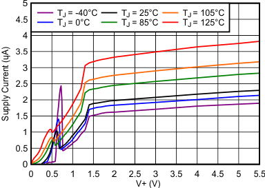
TLV4062 TLV4082 D001_SBVS273.gif
IN1 = IN2 = 1.5 V
Figure 2. Supply Current vs Supply Voltage
TLV4062 TLV4082 D003_SBVS273.gif
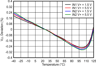
Figure 4. INx Threshold (VIT–) Deviation vs Temperature
TLV4062 TLV4082 D018_SBVS250.gif
V+ = 5.5 V
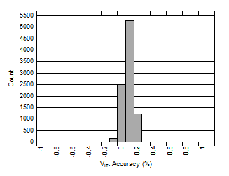
Figure 6. INx Threshold (VIT–)
TLV4062 TLV4082 D005_SBVS273.gif
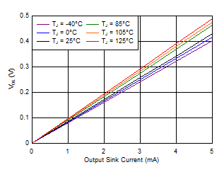
Figure 8. Output Voltage Low vs Output Current
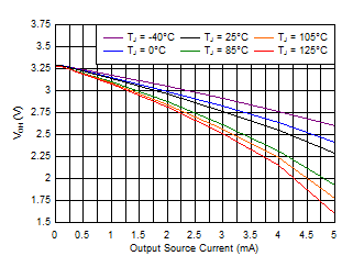
(V+ = 3.3 V)
TLV4062 TLV4082 D007_SBVS273.gif
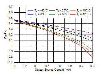
Figure 10. Output Voltage High vs Output Current
(V+ = 1.5 V)
TLV4062 TLV4082 D009_SBVS273.gif
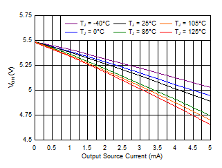
Figure 12. Output Voltage High vs Output Current
(V+ = 5.5 V)
TLV4062 TLV4082 D011_SBVS273.gif
IN1 = IN2 = 1.3 V to 0 V
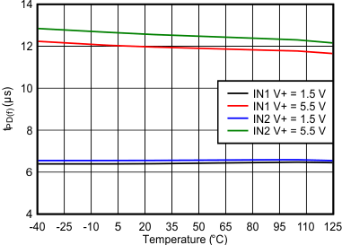
Figure 14. Propagation Delay from
INx Low to Output Low
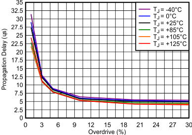
TLV4062 TLV4082 D013_SBVS250.gif
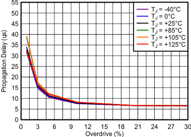
High-to-low transition occurs above the curve
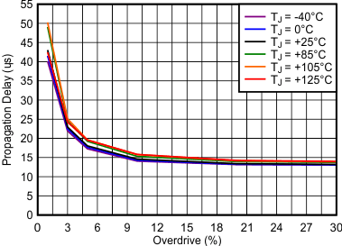
Figure 16. Propagation Delay vs Overdrive
(V+ = 1.5 V)
TLV4062 TLV4082 D015_SBVS250.gif
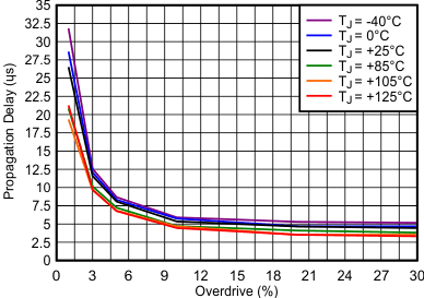
Low-to-high transition occurs above the curve
Figure 18. Propagation Delay vs Overdrive
(V+ = 1.5 V)
TLV4062 TLV4082 D002_SBVS273.gif
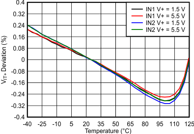
Figure 3. INx Threshold (VIT+) Deviation vs Temperature
TLV4062 TLV4082 D017_SBVS250.gif
V+ = 5.5 V
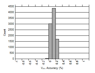
Figure 5. INx Threshold (VIT+)
TLV4062 TLV4082 D004_SBVS273.gif
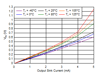
Figure 7. Output Voltage Low vs Output Current
(V+ = 1.5 V)
TLV4062 TLV4082 D006_SBVS273.gif
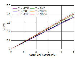
Figure 9. Output Voltage Low vs Output Current
(V+ = 5.5 V)
TLV4062 TLV4082 D008_SBVS273.gif
Figure 11. Output Voltage High vs Output Current
(V+ = 3.3 V)
TLV4062 TLV4082 D010_SBVS273.gif
IN1 = IN2 = 0 V to 1.3 V
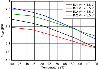
Figure 13. Propagation Delay from
INx High to Output High
TLV4062 TLV4082 D012_SBVS273.gif
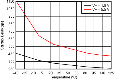
Figure 15. Startup Delay
TLV4062 TLV4082 D014_SBVS250.gif
High-to-low transition occurs above the curve
Figure 17. Propagation Delay vs Overdrive
(V+ = 5.5 V)
TLV4062 TLV4082 D016_SBVS250.gif
Low-to-high transition occurs above the curve
Figure 19. Propagation Delay vs Overdrive
(V+ = 5.5 V)