SBOS533B September   2010  – October 2015 TLV3501A-Q1

PRODUCTION DATA.  

  1. Features
  2. Applications
  3. Description
  4. Revision History
  5. Related Products
  6. Pin Configuration and Functions
  7. Specifications
    1. 7.1 Absolute Maximum Ratings
    2. 7.2 ESD Ratings
    3. 7.3 Recommended Operating Conditions
    4. 7.4 Thermal Information
    5. 7.5 Electrical Characteristics
    6. 7.6 Switching Characteristics
    7. 7.7 Typical Characteristics
  8. Detailed Description
    1. 8.1 Overview
    2. 8.2 Functional Block Diagram
    3. 8.3 Feature Description
      1. 8.3.1 Operating Voltage
      2. 8.3.2 Input Overvoltage Protection
    4. 8.4 Device Functional Modes
      1. 8.4.1 Shutdown
  9. Application and Implementation
    1. 9.1 Application Information
      1. 9.1.1 Adding External Hysteresis
    2. 9.2 Typical Application
      1. 9.2.1 Relaxation Oscillator
        1. 9.2.1.1 Design Requirements
        2. 9.2.1.2 Detailed Design Procedure
        3. 9.2.1.3 Application Curve
      2. 9.2.2 High-Speed Window Comparator
  10. 10Power Supply Recommendations
  11. 11Layout
    1. 11.1 Layout Guidelines
    2. 11.2 Layout Example
  12. 12Device and Documentation Support
    1. 12.1 Documentation Support
      1. 12.1.1 Related Documentation
    2. 12.2 Community Resource
    3. 12.3 Trademarks
    4. 12.4 Electrostatic Discharge Caution
    5. 12.5 Glossary
  13. 13Mechanical, Packaging, and Orderable Information

封装选项

机械数据 (封装 | 引脚)
散热焊盘机械数据 (封装 | 引脚)
订购信息

6 Pin Configuration and Functions

DBV Package
6-Pin SOT-23
Top View
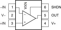
TLV3501A-Q1 po_bos533.gif
Pin 1 is determined by orienting the package marking as indicated on the diagram.

Pin Functions

PIN I/O(1) DESCRIPTION
NO. NAME
1 –IN I Inverting input
2 V– I Negative (lowest) power supply
3 +IN I Noninverting input
4 V+ I Positive (highest) power supply
5 OUT O Output
6 SHDN Shutdown (the device is idle when this pin is not in use)
(1) I = input, O = output