SLCS135B August 2000 – January 2017 TLV3401 , TLV3402 , TLV3404
PRODUCTION DATA.
- 1 Features
- 2 Applications
- 3 Description
- 4 Revision History
- 5 Device Comparison Table
- 6 Pin Configuration and Functions
- 7 Specifications
- 8 Detailed Description
- 9 Application and Implementation
- 10Power Supply Recommendations
- 11Layout
- 12Device and Documentation Support
- 13Mechanical, Packaging, and Orderable Information
封装选项
机械数据 (封装 | 引脚)
散热焊盘机械数据 (封装 | 引脚)
订购信息
7 Specifications
7.1 Absolute Maximum Ratings
over operating free-air temperature range (unless otherwise noted)(1)| MIN | MAX | UNIT | |||
|---|---|---|---|---|---|
| Voltage | Supply, VCC(2) | 17 | V | ||
| Differential input, VID | –20 | 20 | |||
| Input, VI(2)(3) | 0 | VCC + 5 | |||
| Current | Input, II | –10 | 10 | mA | |
| Output, IO | –10 | 10 | |||
| Temperature | Operating, TA | C-suffix versions | 0 | 70 | °C |
| I-suffix versions | –40 | 125 | |||
| Junction, TJ | 150 | ||||
| Storage, Tstg | –65 | 150 | |||
(1) Stresses beyond those listed under Absolute Maximum Ratings may cause permanent damage to the device. These are stress ratings only, which do not imply functional operation of the device at these or any other conditions beyond those indicated under Recommended Operating Conditions. Exposure to absolute-maximum-rated conditions for extended periods may affect device reliability.
(2) All voltage values, except differential voltages, are with respect to GND.
(3) Input voltage range is limited to 20 V or VCC + 5 V, whichever is smaller.
7.2 ESD Ratings
| VALUE | UNIT | |||
|---|---|---|---|---|
| V(ESD) | Electrostatic discharge | Human-body model (HBM), per ANSI/ESDA/JEDEC JS-001(1) | ±2000 | V |
| Charged-device model (CDM), per JEDEC specification JESD22-C101(2) | ±1500 | |||
| Machine model (MM) | ±100 | |||
(1) JEDEC document JEP155 states that 500-V HBM allows safe manufacturing with a standard ESD control process.
7.3 Recommended Operating Conditions
| MIN | MAX | UNIT | |||
|---|---|---|---|---|---|
| Supply voltage, VCC | Single supply | C-suffix versions | 2.5 | 16 | V |
| I-suffix versions | 2.7 | 16 | |||
| Split supply | C-suffix versions | ±1.25 | ±8 | ||
| I-suffix versions | ±1.35 | ±8 | |||
| Common-mode input voltage, VICR | –0.1 | VCC + 5 | V | ||
| Operating free-air temperature, TA | C-suffix versions | 0 | 70 | °C | |
| I-suffix versions | –40 | 125 | |||
7.4 Thermal Information: TLV3401
| THERMAL METRIC(1) | TLV3401 | UNIT | |||
|---|---|---|---|---|---|
| D (SOIC) | DBV (SOT-23) | P (PDIP) | |||
| 8 PINS | 5 PINS | 8 PINS | |||
| RθJA | Junction-to-ambient thermal resistance | 201.9 | 237.8 | 58.5 | °C/W |
| RθJC(top) | Junction-to-case (top) thermal resistance | 92.5 | 108.7 | 48.3 | °C/W |
| RθJB | Junction-to-board thermal resistance | 123.3 | 64.1 | 35.6 | °C/W |
| ψJT | Junction-to-top characterization parameter | 23 | 12.1 | 25.9 | °C/W |
| ψJB | Junction-to-board characterization parameter | 212.6 | 63.3 | 35.5 | °C/W |
| RθJC(bot) | Junction-to-case (bottom) thermal resistance | — | — | — | °C/W |
7.5 Thermal Information: TLV3402
| THERMAL METRIC(1) | TLV3402 | UNIT | |||
|---|---|---|---|---|---|
| D (SOIC) | DGK (VSSOP) | P (PDIP) | |||
| 8 PINS | 8 PINS | 8 PINS | |||
| RθJA | Junction-to-ambient thermal resistance | 201.9 | 186.8 | 58.5 | °C/W |
| RθJC(top) | Junction-to-case (top) thermal resistance | 92.5 | 77.5 | 48.3 | °C/W |
| RθJB | Junction-to-board thermal resistance | 123.3 | 107.8 | 35.6 | °C/W |
| ψJT | Junction-to-top characterization parameter | 23 | 15.7 | 25.9 | °C/W |
| ψJB | Junction-to-board characterization parameter | 212.6 | 106.2 | 35.5 | °C/W |
| RθJC(bot) | Junction-to-case (bottom) thermal resistance | — | — | — | °C/W |
(1) For more information about traditional and new thermal metrics, see the application report, Semiconductor and IC Package Thermal Metrics
7.6 Thermal Information: TLV3404
| THERMAL METRIC(1) | TLV3404 | UNIT | |||
|---|---|---|---|---|---|
| D (SOIC) | N (PDIP) | PW (TSSOP) | |||
| 14 PINS | 14 PINS | 14 PINS | |||
| RθJA | Junction-to-ambient thermal resistance | 83.8 | 65.5 | 120.8 | °C/W |
| RθJC(top) | Junction-to-case (top) thermal resistance | 70.7 | 20.0 | 34.3 | °C/W |
| RθJB | Junction-to-board thermal resistance | 59.5 | 25.9 | 62.8 | °C/W |
| ψJT | Junction-to-top characterization parameter | 11.6 | 1.9 | 1 | °C/W |
| ψJB | Junction-to-board characterization parameter | 37.7 | 25.3 | 56.5 | °C/W |
| RθJC(bot) | Junction-to-case (bottom) thermal resistance | — | — | — | °C/W |
7.7 Electrical Characteristics
At specified free-air temperature and VCC = 2.7 V, 5 V, 15 V, unless otherwise noted.| PARAMETER | TEST CONDITIONS | TA(1) | MIN | TYP | MAX | UNIT | ||
|---|---|---|---|---|---|---|---|---|
| DC PERFORMANCE | ||||||||
| VIO | Input offset voltage | VIC = VCC/2, RS = 50 Ω, RP = 1 MΩ | TA = 25°C | 250 | 3600 | µV | ||
| Full range | 4400 | |||||||
| αVIO | Offset voltage drift | VIC = VCC/2, RS = 50 Ω, RP = 1 MΩ | TA = 25°C | 3 | µV/°C | |||
| CMRR | Common-mode rejection ratio | VIC = 0 V to 2.7 V, RS = 50 Ω | TA = 25°C | 55 | 72 | dB | ||
| Full range | 50 | |||||||
| VIC = 0 V to 5 V, RS = 50 Ω | TA = 25°C | 60 | 76 | |||||
| Full range | 55 | |||||||
| VIC = 0 V to 15 V, RS = 50 Ω | TA = 25°C | 65 | 88 | |||||
| Full range | 60 | |||||||
| AVD | Large-signal differential voltage amplification | RP = 1 MΩ | TA = 25°C | 1000 | V/mV | |||
| INPUT/OUTPUT CHARACTERISTICS | ||||||||
| IIO | Input offset current | VIC = VCC/2, RS = 50 Ω, RP = 1 MΩ | TA = 25°C | 20 | 100 | pA | ||
| Full range | 1000 | |||||||
| IIB | Input bias current | VIC = VCC/2, RS = 50 Ω, RP = 1 MΩ | TA = 25°C | 80 | 250 | pA | ||
| Full range | 1500 | |||||||
| ri(d) | Differential input resistance | TA = 25°C | 300 | MΩ | ||||
| IOZ | High-impedance output leakage current | VIC = VCC/2, VO = VCC, VID = 1 V | TA = 25°C | 50 | pA | |||
| VOL | Low-level output voltage | VIC = VCC/2, IOL = 2 µA, VID = –1 V | TA = 25°C | 8 | mV | |||
| VIC = VCC/2, IOL = 50 µA, VID = –1 V | TA = 25°C | 80 | 200 | |||||
| Full range | 300 | |||||||
| POWER SUPPLY | ||||||||
| ICC | Supply current (per channel) | RP = no pullup | Output state low | TA = 25°C | 470 | 550 | nA | |
| Full range | 750 | |||||||
| Output state high | TA = 25°C | 560 | 640 | |||||
| Full range | 950 | |||||||
| PSRR | Power-supply rejection ratio | VIC = VCC/2, no load | VCC = 2.7 V to 5 V |
TA = 25°C | 75 | 100 | dB | |
| Full range | 70 | |||||||
| VCC = 5 V to 15 V | TA = 25°C | 85 | 105 | |||||
| Full range | 80 | |||||||
(1) Full range is 0°C to 70°C for the C-suffix and –40°C to 125°C for the I-suffix. If not specified, full range is –40°C to 125°C.
7.8 Switching Characteristics
At TA = 25°C, recommended operating conditions, and VCC = 2.7 V, 5 V, 15 V, unless otherwise noted.| PARAMETER | TEST CONDITIONS | TA | MIN | TYP | MAX | UNIT | ||
|---|---|---|---|---|---|---|---|---|
| t(PLH) | Propagation delay time, low-to-high-level output | f = 10 kHz, VSTEP = 1 V, RP = 1 MΩ, CL = 10 pF |
Overdrive = 2 mV | TA = 25°C | 175 | µs | ||
| Overdrive = 10 mV | TA = 25°C | 80 | ||||||
| Overdrive = 50 mV | TA = 25°C | 55 | ||||||
| t(PHL) | Propagation delay time, high-to-low-level output | f = 10 kHz, VSTEP = 1 V, RP = 1 MΩ, CL = 10 pF |
Overdrive = 2 mV | TA = 25°C | 300 | µs | ||
| Overdrive = 10 mV | TA = 25°C | 60 | ||||||
| Overdrive = 50 mV | TA = 25°C | 30 | ||||||
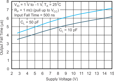
| tF | Fall time | RP = 1 MΩ, CL = 10 pF | TA = 25°C | 5 | µs | |||
7.9 Typical Characteristics
Table 1. Table of Graphs
| DESCRIPTION | FIGURE NO. | ||
|---|---|---|---|
| Input bias/offset current | vs Free-air temperature | Figure 1 | |
| Open collector leakage current | vs Free-air temperature | Figure 2 | |
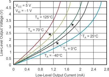
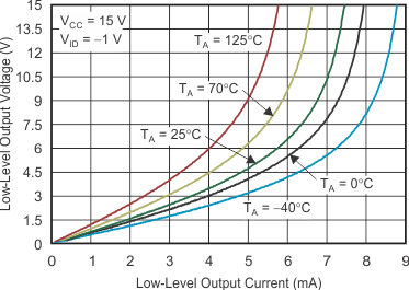
| VOL | Low-level output voltage | vs Low-level output current | Figure 3, Figure 4, Figure 5 |
| IDD | Supply current | vs Supply voltage | Figure 6 |
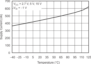
| IDD | Supply current | vs Free-air temperature | Figure 7 |
| Low-to-high level output response for various input overdrives | Figure 8, Figure 9, Figure 10 | ||
| High-to-low level output response for various input overdrives | Figure 11, Figure 12, Figure 13 | ||
| Output fall time | vs Supply voltage | Figure 14 | |
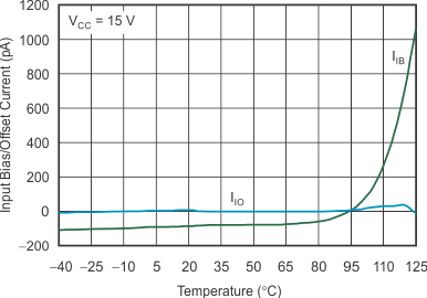
Free-Air Temperature
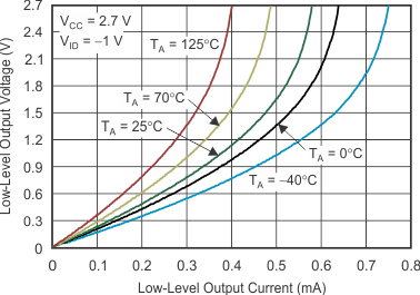
Low-Level Output Current
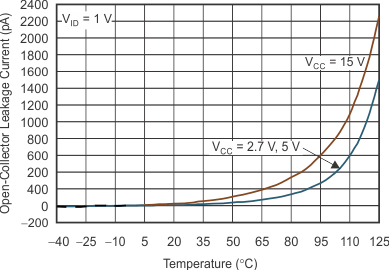
Free-Air Temperature
Low-Level Output Current
Low-Level Output Current
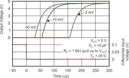
for Various Input Overdrives
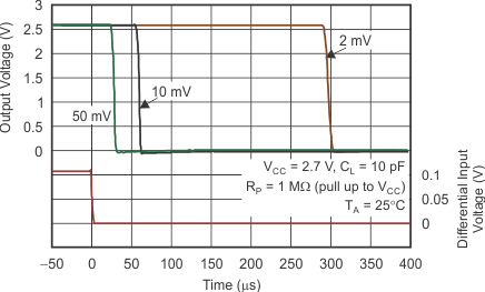
for Various Input Overdrives
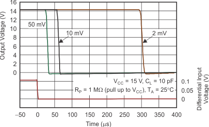
for Various Input Overdrives
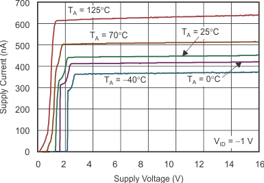
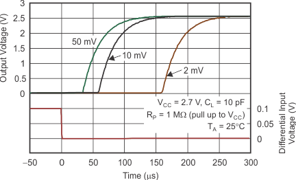
for Various Input Overdrives
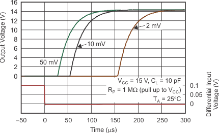
for Various Input Overdrives
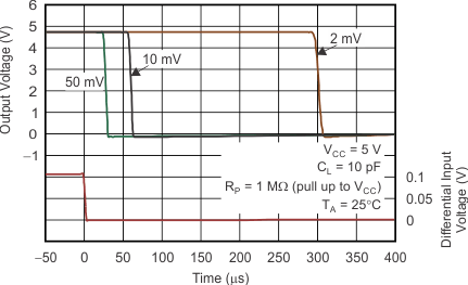
for Various Input Overdrives
