ZHCSOF3G April   2006  – July 2021 TLV320AIC3106

PRODUCTION DATA  

  1. 特性
  2. 应用
  3. 说明
  4. Revision History
  5. 说明(续)
  6. Device Comparison Table
  7. Pin Configuration and Functions
  8. Specifications
    1. 8.1 Absolute Maximum Ratings
    2. 8.2 ESD Ratings
    3. 8.3 Recommended Operating Conditions
    4. 8.4 Thermal Information
    5. 8.5 Electrical Characteristics
    6. 8.6 Timing Requirements: Audio Data Serial Interface (1)
    7. 8.7 Timing Diagrams
    8. 8.8 Typical Characteristics
  9. Parameter Measurement Information
  10. 10Detailed Description
    1. 10.1 Overview
    2. 10.2 Functional Block Diagram
    3. 10.3 Feature Description
      1. 10.3.1  Hardware Reset
      2. 10.3.2  Digital Audio Data Serial Interface
        1. 10.3.2.1 Right-Justified Mode
        2. 10.3.2.2 Left-Justified Mode
        3. 10.3.2.3 I2S Mode
        4. 10.3.2.4 DSP Mode
        5. 10.3.2.5 TDM Data Transfer
      3. 10.3.3  Audio Data Converters
        1. 10.3.3.1 Audio Clock Generation
        2. 10.3.3.2 Stereo Audio ADC
          1. 10.3.3.2.1 Stereo Audio ADC High-Pass Filter
          2. 10.3.3.2.2 Automatic Gain Control (AGC)
            1. 10.3.3.2.2.1 Target Level
            2. 10.3.3.2.2.2 Attack Time
            3. 10.3.3.2.2.3 Decay Time
            4. 10.3.3.2.2.4 Noise Gate Threshold
            5. 10.3.3.2.2.5 Maximum PGA Gain Applicable
        3. 10.3.3.3 Stereo Audio DAC
          1. 10.3.3.3.1 Digital Audio Processing for Playback
          2. 10.3.3.3.2 Digital Interpolation Filter
          3. 10.3.3.3.3 Delta-Sigma Audio DAC
          4. 10.3.3.3.4 Audio DAC Digital Volume Control
          5. 10.3.3.3.5 Increasing DAC Dynamic Range
          6. 10.3.3.3.6 Analog Output Common-Mode Adjustment
          7. 10.3.3.3.7 Audio DAC Power Control
      4. 10.3.4  Audio Analog Inputs
      5. 10.3.5  Analog Fully Differential Line Output Drivers
      6. 10.3.6  Analog High Power Output Drivers
      7. 10.3.7  Input Impedance and VCM Control
      8. 10.3.8  General-Purpose I/O
      9. 10.3.9  Digital Microphone Connectivity
      10. 10.3.10 Micbias Generation
      11. 10.3.11 Short Circuit Output Protection
      12. 10.3.12 Jack/Headset Detection
    4. 10.4 Device Functional Modes
      1. 10.4.1 Bypass Path Mode
        1. 10.4.1.1 Analog Input Bypass Path Functionality
        2. 10.4.1.2 ADC PGA Signal Bypass Path Functionality
        3. 10.4.1.3 Passive Analog Bypass During Powerdown
      2. 10.4.2 Digital Audio Processing for Record Path
    5. 10.5 Programming
      1. 10.5.1 Digital Control Serial Interface
        1. 10.5.1.1 SPI Control Mode
          1. 10.5.1.1.1 SPI Communication Protocol
          2. 10.5.1.1.2 Limitation on Register Writing
          3. 10.5.1.1.3 Continuous Read / Write Operation
        2. 10.5.1.2 I2C Control Interface
          1. 10.5.1.2.1 I2C BUS Debug in a Glitched System
    6. 10.6 Register Maps
      1. 10.6.1 Output Stage Volume Controls
  11. 11Application and Implementation
    1. 11.1 Application Information
    2. 11.2 Typical Application
      1. 11.2.1 Design Requirements
      2. 11.2.2 Detailed Design Procedure
      3. 11.2.3 Application Curves
  12. 12Power Supply Recommendations
  13. 13Layout
    1. 13.1 Layout Guidelines
    2. 13.2 Layout Examples
  14. 14Device and Documentation Support
    1. 14.1 接收文档更新通知
    2. 14.2 支持资源
    3. 14.3 Trademarks
    4. 14.4 Electrostatic Discharge Caution
    5. 14.5 术语表

封装选项

请参考 PDF 数据表获取器件具体的封装图。

机械数据 (封装 | 引脚)
  • RGZ|48
  • ZXH|80
散热焊盘机械数据 (封装 | 引脚)
订购信息
Stereo Audio ADC High-Pass Filter

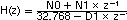
Often in audio applications it is desirable to remove the dc offset from the converted audio data stream. The TLV320AIC3106 has a programmable first-order high-pass filter which can be used for this purpose. The digital filter coefficients are in 16-bit format and therefore use two 8-bit registers for each of the three coefficients, N0, N1, and D1. The transfer function of the digital high-pass filter is of the form:

Equation 5. GUID-4E594427-729B-45B9-8FC0-C24B7E770BBA-low.gif

Programming the left channel is done by writing to page 1, registers 65–70, and the right channel is programmed by writing to page 1, registers 71–76. After the coefficients have been loaded, these ADC high-pass filter coefficients can be selected by writing to page 0, register 107, bits D7–D6, and the high-pass filter can be enabled by writing to page 0, register 12, bits D7–D4.