SLAS513C February   2007  – December 2014 TLV320AIC3105

PRODUCTION DATA.  

  1. Features
  2. Applications
  3. Description
  4. Revision History
  5. Description (Continued)
  6. Related Devices
  7. Pin Configuration and Functions
  8. Specifications
    1. 8.1 Absolute Maximum Ratings
    2. 8.2 ESD Ratings
    3. 8.3 Recommended Operating Conditions
    4. 8.4 Thermal Information
    5. 8.5 Electrical Characteristics
    6. 8.6 Audio Data Serial Interface Timing Requirements
    7. 8.7 Typical Characteristics
  9. Parameter Measurement Information
  10. 10Detailed Description
    1. 10.1 Overview
    2. 10.2 Functional Block Diagram
    3. 10.3 Feature Description
      1. 10.3.1  Hardware Reset
      2. 10.3.2  Digital Control Serial Interface
        1. 10.3.2.1 Right-Justified Mode
        2. 10.3.2.2 Left-Justified Mode
        3. 10.3.2.3 I2S Mode
        4. 10.3.2.4 DSP Mode
        5. 10.3.2.5 TDM Data Transfer
      3. 10.3.3  Audio Data Converters
        1. 10.3.3.1 Audio Clock Generation
        2. 10.3.3.2 Stereo Audio ADC
          1. 10.3.3.2.1 Stereo Audio ADC High-Pass Filter
          2. 10.3.3.2.2 Automatic Gain Control (AGC)
            1. 10.3.3.2.2.1 Target Level
            2. 10.3.3.2.2.2 Attack Time
            3. 10.3.3.2.2.3 Decay Time
            4. 10.3.3.2.2.4 Noise Gate Threshold
            5. 10.3.3.2.2.5 Maximum PGA Gain Applicable
        3. 10.3.3.3 Stereo Audio DAC
          1. 10.3.3.3.1 Digital Audio Processing for Playback
          2. 10.3.3.3.2 Digital Interpolation Filter
          3. 10.3.3.3.3 Delta-Sigma Audio DAC
          4. 10.3.3.3.4 Audio DAC Digital Volume Control
          5. 10.3.3.3.5 Increasing DAC Dynamic Range
          6. 10.3.3.3.6 Analog Output Common-Mode Adjustment
          7. 10.3.3.3.7 Audio DAC Power Control
      4. 10.3.4  Audio Analog Inputs
      5. 10.3.5  Analog Fully Differential Line Output Drivers
      6. 10.3.6  Analog High-Power Output Drivers
      7. 10.3.7  Input Impedance and VCM Control
      8. 10.3.8  MICBIAS Generation
      9. 10.3.9  Short-Circuit Output Protection
      10. 10.3.10 Jack and Headset Detection
    4. 10.4 Device Functional Modes
      1. 10.4.1 Bypass Path Mode
        1. 10.4.1.1 Analog Input Bypass Path Functionality
        2. 10.4.1.2 ADC PGA Signal Bypass Path Functionality
        3. 10.4.1.3 Passive Analog Bypass During Power Down
      2. 10.4.2 Digital Audio Processing for Record Path
    5. 10.5 Programming
      1. 10.5.1 I2C Control Interface
        1. 10.5.1.1 I2C Bus Debug in a Glitched System
      2. 10.5.2 Register Map Structure
    6. 10.6 Register Maps
      1. 10.6.1 Control Registers
      2. 10.6.2 Output Stage Volume Controls
  11. 11Application and Implementation
    1. 11.1 Application Information
    2. 11.2 Typical Applications
      1. 11.2.1 Capless Headphone and External Speaker Amp
        1. 11.2.1.1 Design Requirements
        2. 11.2.1.2 Detailed Design Procedure
        3. 11.2.1.3 Application Curves
      2. 11.2.2 AC-Coupled Headphone Out With Separate Line Outputs and External Speaker Amplifier
        1. 11.2.2.1 Design Requirements
        2. 11.2.2.2 Detailed Design Procedure
        3. 11.2.2.3 Application Curves
  12. 12Power Supply Recommendations
  13. 13Layout
    1. 13.1 Layout Guidelines
    2. 13.2 Layout Example
  14. 14Device and Documentation Support
    1. 14.1 Trademarks
    2. 14.2 Electrostatic Discharge Caution
    3. 14.3 Glossary
  15. 15Mechanical, Packaging, and Orderable Information

封装选项

机械数据 (封装 | 引脚)
散热焊盘机械数据 (封装 | 引脚)
订购信息

12 Power Supply Recommendations

The TLV320AIC3105 has been designed to be extremely tolerant of power supply sequencing. However, in some rare instances, unexpected conditions can be attributed to power supply sequencing. The following sequence will provide the most robust operation.

IOVDD should be powered up first. The analog supplies, which include AVDD and DRVDD, should be powered up second. The digital supply DVDD should be powered up last. Keep RESET low until all supplies are stable. The analog supplies should be greater than or equal to DVDD at all times.

TLV320AIC31xx_ Power_ Supply_Sequencing.png
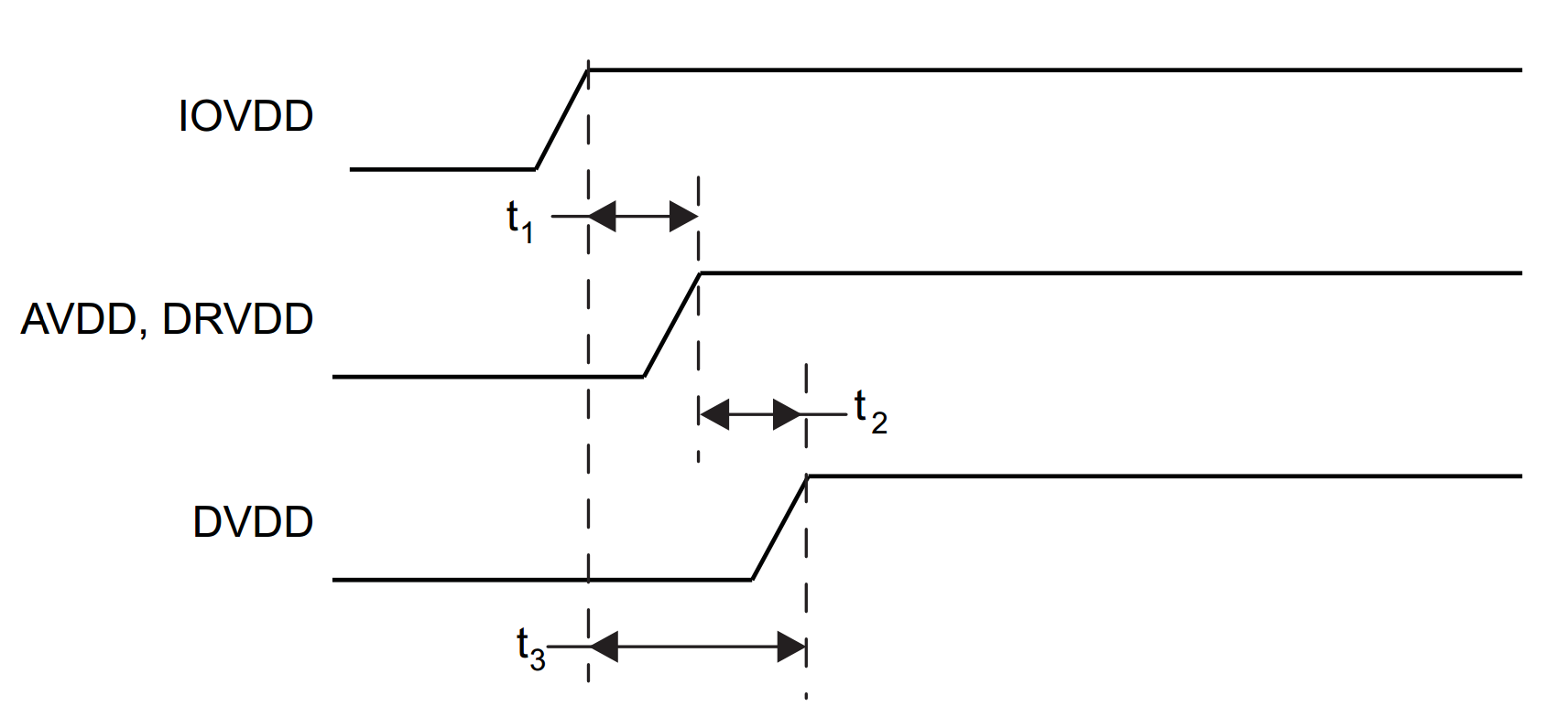
Figure 37. TLV320AIC3105 Power Supply Sequencing
SYMBOL PARAMETER MIN MAX UNIT
t1 IOVDD to AVDD, DRVDD 0 ms
t2 AVDD to DVDD 0 4
t3 IOVDD to DVDD 0