SLAS513C February 2007 – December 2014 TLV320AIC3105
PRODUCTION DATA.
- 1 Features
- 2 Applications
- 3 Description
- 4 Revision History
- 5 Description (Continued)
- 6 Related Devices
- 7 Pin Configuration and Functions
- 8 Specifications
- 9 Parameter Measurement Information
-
10Detailed Description
- 10.1 Overview
- 10.2 Functional Block Diagram
- 10.3
Feature Description
- 10.3.1 Hardware Reset
- 10.3.2 Digital Control Serial Interface
- 10.3.3 Audio Data Converters
- 10.3.4 Audio Analog Inputs
- 10.3.5 Analog Fully Differential Line Output Drivers
- 10.3.6 Analog High-Power Output Drivers
- 10.3.7 Input Impedance and VCM Control
- 10.3.8 MICBIAS Generation
- 10.3.9 Short-Circuit Output Protection
- 10.3.10 Jack and Headset Detection
- 10.4 Device Functional Modes
- 10.5 Programming
- 10.6 Register Maps
- 11Application and Implementation
- 12Power Supply Recommendations
- 13Layout
- 14Device and Documentation Support
- 15Mechanical, Packaging, and Orderable Information
10 Detailed Description
10.1 Overview
The TLV320AIC3105 is a highly flexible, low-power, stereo audio codec with extensive feature integration, intended for applications in smartphones, PDAs, and portable computing, communication, and entertainment applications. Available in a 5-mm × 5-mm, 32-lead QFN, the product integrates a host of features to reduce cost, board space, and power consumption in space-constrained, battery-powered, portable applications.
The TLV320AIC3105 consists of the following blocks:
- Stereo audio multibit delta-sigma DAC (8 kHz–96 kHz)
- Stereo audio multibit delta-sigma ADC (8 kHz–96 kHz)
- Programmable digital audio effects processing (3-D, bass, treble, midrange, EQ, notch filter, de-emphasis)
- Six audio inputs
- Four high-power audio output drivers (headphone drive capability)
- Two fully differential line output drivers
- Fully programmable PLL
- Headphone/headset jack detection available as register status bit
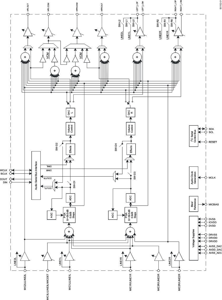
10.2 Functional Block Diagram
10.3 Feature Description
10.3.1 Hardware Reset
The TLV320AIC3105 requires a hardware reset after power up for proper operation. After all power supplies are at their specified values, the RESET pin must be driven low for at least 10 ns. If this reset sequence is not performed, the TLV320AIC3105 may not respond properly to register reads/writes.
10.3.2 Digital Control Serial Interface
The register map of the TLV320AIC3105 actually consists of multiple pages of registers, with each page containing 128 registers. The register at address zero on each page is used as a page-control register, and writing to this register determines the active page for the device. All subsequent read/write operations access the page that is active at the time, unless a register write is performed to change the active page. Only two pages of registers are implemented in this product, with the active page defaulting to page 0 on device reset.
For example, at device reset, the active page defaults to page 0, and thus all register read/write operations for addresses 1 to 127 access registers in page 0. If registers on page 1 must be accessed, the user must write the 8-bit sequence 0x01 to register 0, the page control register, to change the active page from page 0 to page 1. After this write, it is recommended the user also read back the page control register, to safely ensure the change in page control has occurred properly. Future read/write operations to addresses 1 to 127 now access registers in page 1. When page-0 registers must be accessed again, the user writes the 8-bit sequence 0x00 to register 0, the page control register, to change the active page back to page 0. After a recommended read of the page control register, all further read/write operations to addresses 1 to 127 access page-0 registers again.
10.3.2.1 Right-Justified Mode
In right-justified mode, the LSB of the left channel is valid on the rising edge of the bit clock preceding the falling edge of word clock. Similarly, the LSB of the right channel is valid on the rising edge of the bit clock preceding the rising edge of the word clock.
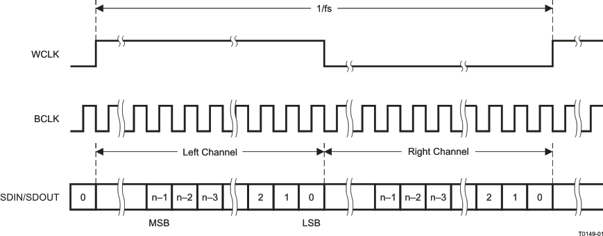 Figure 12. Right-Justified Serial Data Bus Mode Operation
10.3.2.2 Left-Justified Mode
In left-justified mode, the MSB of the right channel is valid on the rising edge of the bit clock following the falling edge of the word clock. Similarly the MSB of the left channel is valid on the rising edge of the bit clock following the rising edge of the word clock.
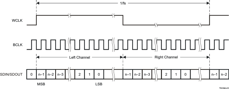 Figure 13. Left-Justified Serial Data Bus Mode Operation
10.3.2.3 I2S Mode
In I2S mode, the MSB of the left channel is valid on the second rising edge of the bit clock after the falling edge of the word clock. Similarly the MSB of the right channel is valid on the second rising edge of the bit clock after the rising edge of the word clock.
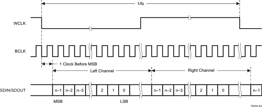 Figure 14. I2S Serial Data Bus Mode Operation
10.3.2.4 DSP Mode
In DSP mode, the rising edge of the word clock starts the data transfer with the left-channel data first and immediately followed by the right-channel data. Each data bit is valid on the falling edge of the bit clock.
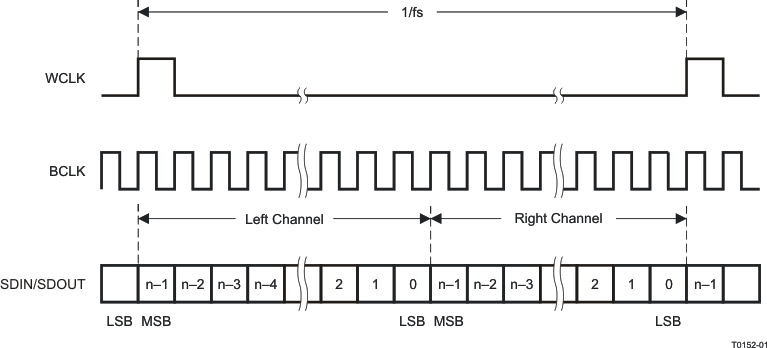 Figure 15. DSP Serial Data Bus Mode Operation
10.3.2.5 TDM Data Transfer
Time-division multiplexed data transfer can be realized in any of the above transfer modes if the 256-clock bit-clock mode is selected, although it is recommended to be used in either left-justified mode or DSP mode. By changing the programmable offset, the bit clock in each frame where the data begins can be changed, and the serial data output driver (DOUT) can also be programmed to the high-impedance state during all bit clocks except when valid data is being put onto the bus. This allows other codecs to be programmed with different offsets and to drive their data onto the same DOUT line, just in a different slot. For incoming data, the codec simply ignores data on the bus except where it is expected based on the programmed offset.
Note that the location of the data when an offset is programmed is different, depending on what transfer mode is selected. In DSP mode, both left and right channels of data are transferred immediately adjacent to each other in the frame. This differs from left-justified mode, where the left- and right-channel data are always a half-frame apart in each frame. In this case, as the offset is programmed from zero to some higher value, both the left- and right-channel data move across the frame, but still stay a full half-frame apart from each other. This is depicted in Figure 16 for the two cases.
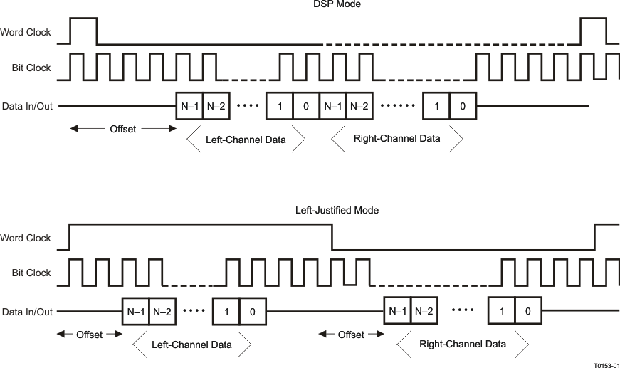 Figure 16. DSP Mode and Left-Justified Modes, Showing the
 Effect of a Programmed Data Word Offset
10.3.3 Audio Data Converters
The TLV320AIC3105 supports the following standard audio sampling rates: 8 kHz, 11.025 kHz, 12 kHz, 16 kHz, 22.05 kHz, 24 kHz, 32 kHz, 44.1 kHz, 48 kHz, 88.2 kHz, and 96 kHz. The converters can also operate at different sampling rates in various combinations, which are described further below.
The data converters are based on the concept of an fS(ref) rate that is used internal to the part, and it is related to the actual sampling rates of the converters through a series of ratios. For typical sampling rates, fS(ref) is either 44.1 kHz or 48 kHz, although it can realistically be set over a wider range of rates up to 53 kHz, with additional restrictions applying if the PLL is used. This concept is used to set the sampling rates of the ADC and DAC, and also to enable high quality playback of low sampling rate data, without high frequency audible noise being generated.
The sampling rate of the ADC and DAC can be set to fS(ref)/NDAC or 2 × fS(ref)/NDAC, with NDAC being 1, 1.5, 2, 2.5, 3, 3.5, 4, 4.5, 5, 5.5, or 6 for both the NDAC and NADC settings. In the TLV320AIC3105, the NDAC and NADC should be set to the same value, as the device only supports a common sample rate for the ADC and DAC channels. Therefore, NCODEC = NDAC = NDAC, and this is programmed by setting the value of bits D7–D4 equal to the value of bits D3–D0 in page 0, register 2.
10.3.3.1 Audio Clock Generation
The audio converters in the TLV320AIC3105 need an internal audio master clock at a frequency of 256 × fS(ref), which can be obtained in a variety of manners from an external clock signal applied to the device.
A more detailed diagram of the audio clock section of the TLV320AIC3105 is shown in Figure 17.
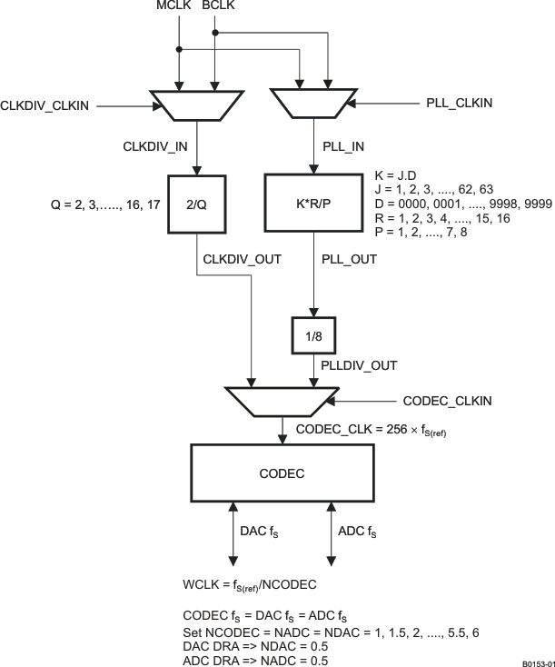 Figure 17. Audio Clock Generation Processing
The part can accept an MCLK input from 512 kHz to 50 MHz, which can then be passed through either a programmable divider or a PLL, to get the proper internal audio master clock needed by the part. The BCLK input can also be used to generate the internal audio master clock.
A primary concern is proper operation of the codec at various sample rates with the limited MCLK frequencies available in the system. This device includes a highly programmable PLL to accommodate such situations easily. The integrated PLL can generate audio clocks from a wide variety of possible MCLK inputs, with particular focus paid to the standard MCLK rates already widely used.
When the PLL is disabled,
fS(ref) = CLKDIV_IN/(128 × Q)
Where Q = 2, 3, …, 17
CLKDIV_IN can be MCLK or BCLK, selected by register 102, bits D7–D6.
NOTE – when NDAC = 1.5, 2.5, 3.5, 4.5, or 5.5, odd values of Q are not allowed. In this mode, MCLK can be as high as 50 MHz, and fS(ref) should fall within 39 kHz to 53 kHz. (In the TLV320AIC3105, the NDAC setting must be the same as the NADC setting. The NDAC ratio is set on page 0, register 2. The NDAC is set equal to NADC by setting the value of bits D7–D4 equal to that of bits D3–D0.)
When the PLL is enabled,
fS(ref) = (PLLCLK_IN × K × R)/(2048 × P), where
P = 1, 2, 3,…, 8
R = 1, 2, …, 16
K = J.D
J = 1, 2, 3, …, 63
D = 0000, 0001, 0002, 0003, …, 9998, 9999
PLLCLK_IN can be MCLK or BCLK, selected by page 0, register 102, bits D5–D4
P, R, J, and D are register programmable. J is the integer portion of K (the numbers to the left of the decimal point), while D is the fractional portion of K (the numbers to the right of the decimal point, assuming four digits of precision).
Examples:
If K = 8.5, then J = 8, D = 5000
If K = 7.12, then J = 7, D = 1200
If K = 14.03, then J = 14, D = 0300
If K = 6.0004, then J = 6, D = 0004
When the PLL is enabled and D = 0000, the following conditions must be satisfied to meet specified performance:
2 MHz ≤ ( PLLCLK_IN/P ) ≤ 20 MHz
80 MHz ≤ (PLLCLK _IN × K × R/P ) ≤ 110 MHz
4 ≤ J ≤ 55
When the PLL is enabled and D≠0000, the following conditions must be satisfied to meet specified performance:
10 MHz ≤ PLLCLK _IN/P ≤ 20 MHz
80 MHz ≤ PLLCLK _IN × K × R/P ≤ 110 MHz
4 ≤ J ≤ 11
R = 1
Example:
MCLK = 12 MHz and fS(ref) = 44.1 kHz
Select P = 1, R = 1, K = 7.5264, which results in J = 7, D = 5264
Example:
MCLK = 12 MHz and fS(ref) = 48 kHz
Select P = 1, R = 1, K = 8.192, which results in J = 8, D = 1920
The table below lists several example cases of typical MCLK rates and how to program the PLL to achieve fS(ref) = 44.1 kHz or 48 kHz.
| MCLK (MHz) | P | R | J | D | ACHIEVED fS(ref) | % ERROR |
|---|---|---|---|---|---|---|
| fS(ref) = 44.1 kHz | ||||||
| 2.8224 | 1 | 1 | 32 | 0 | 44,100 | 0 |
| 5.6448 | 1 | 1 | 16 | 0 | 44,100 | 0 |
| 12 | 1 | 1 | 7 | 5264 | 44,100 | 0 |
| 13 | 1 | 1 | 6 | 9474 | 44,099.71 | –0.0007 |
| 16 | 1 | 1 | 5 | 6448 | 44,100 | 0 |
| 19.2 | 1 | 1 | 4 | 7040 | 44,100 | 0 |
| 19.68 | 1 | 1 | 4 | 5893 | 44,100.30 | 0.0007 |
| 48 | 4 | 1 | 7 | 5264 | 44,100 | 0 |
| fS(ref) = 48 kHz | ||||||
| 2.048 | 1 | 1 | 48 | 0 | 48,000 | 0 |
| 3.072 | 1 | 1 | 32 | 0 | 48,000 | 0 |
| 4.096 | 1 | 1 | 24 | 0 | 48,000 | 0 |
| 6.144 | 1 | 1 | 16 | 0 | 48,000 | 0 |
| 8.192 | 1 | 1 | 12 | 0 | 48,000 | 0 |
| 12 | 1 | 1 | 8 | 1920 | 48,000 | 0 |
| 13 | 1 | 1 | 7 | 5618 | 47,999.71 | –0.0006 |
| 16 | 1 | 1 | 6 | 1440 | 48,000 | 0 |
| 19.2 | 1 | 1 | 5 | 1200 | 48,000 | 0 |
| 19.68 | 1 | 1 | 4 | 9951 | 47,999.79 | –0.0004 |
| 48 | 4 | 1 | 8 | 1920 | 48,000 | 0 |
10.3.3.2 Stereo Audio ADC
The TLV320AIC3105 includes a stereo audio ADC, which uses a delta-sigma modulator with 128-times oversampling in single-rate mode, followed by a digital decimation filter. The ADC supports sampling rates from 8 kHz to 48 kHz in single-rate mode, and up to 96 kHz in dual-rate mode. Whenever the ADC or DAC is in operation, the device requires that an audio master clock be provided and appropriate audio clock generation be set up within the device.
In order to provide optimal system power dissipation, the stereo ADC can be powered one channel at a time, to support the case where only mono record capability is required. In addition, both channels can be fully powered or entirely powered down.
The integrated digital decimation filter removes high-frequency content and down-samples the audio data from an initial sampling rate of 128 fS to the final output sampling rate of fS. The decimation filter provides a linear phase output response with a group delay of 17/fS. The –3-dB bandwidth of the decimation filter extends to 0.45 fS and scales with the sample rate (fS). The filter has minimum 75-dB attenuation over the stop band from 0.55 fS to 64 fS. Independent digital high-pass filters are also included with each ADC channel, with a corner frequency that can be independently set.
Because of the oversampling nature of the audio ADC and the integrated digital decimation filtering, requirements for analog antialiasing filtering are very relaxed. The TLV320AIC3105 integrates a second-order analog antialiasing filter with 20-dB attenuation at 1 MHz. This filter, combined with the digital decimation filter, provides sufficient antialiasing filtering without requiring additional external components.
The ADC is preceded by a programmable gain amplifier (PGA), which allows analog gain control from 0 dB to 59.5 dB in steps of 0.5 dB. The PGA gain changes are implemented with an internal soft-stepping algorithm that only changes the actual volume level by one 0.5-dB step every one or two ADC output samples, depending on the register programming (see page 0, registers 19 and 22). This soft-stepping ensures that volume control changes occur smoothly with no audible artifacts. On reset, the PGA gain defaults to a mute condition, and on power down, the PGA soft-steps the volume to mute before shutting down. A read-only flag is set whenever the gain applied by PGA equals the desired value set by the register. The soft-stepping control can also be disabled by programming a register bit. When soft stepping is enabled, the audio master clock must be applied to the part after the ADC power-down register is written to ensure the soft-stepping to mute has completed. When the ADC power-down flag is no longer set, the audio master clock can be shut down.
10.3.3.2.1 Stereo Audio ADC High-Pass Filter
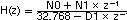
Often in audio applications it is desirable to remove the dc offset from the converted audio data stream. The TLV320AIC3105 has a programmable first-order high-pass filter which can be used for this purpose. The digital filter coefficients are in 16-bit format and therefore use two 8-bit registers for each of the three coefficients, N0, N1, and D1. The transfer function of the digital high-pass filter is of the form:
Programming the left channel is done by writing to page 1, registers 65–70, and the right channel is programmed by writing to page 1, registers 71–76. After the coefficients have been loaded, these ADC high-pass filter coefficients can be selected by writing to page 0, register 107, bits D7–D6, and the high-pass filter can be enabled by writing to page 0, register 12, bits D7–D4.
10.3.3.2.2 Automatic Gain Control (AGC)
An automatic gain control (AGC) circuit is included with the ADC and can be used to maintain nominally constant output signal amplitude when recording speech signals (it can be fully disabled if not desired). This circuitry automatically adjusts the PGA gain as the input signal becomes overly loud or very weak, such as when a person speaking into a microphone moves closer or farther from the microphone. The AGC algorithm has several programmable settings, including target gain, attack and decay time constants, noise threshold, and maximum PGA gain applicable that allow the algorithm to be fine tuned for any particular application. The algorithm uses the absolute average of the signal (which is the average of the absolute value of the signal) as a measure of the nominal amplitude of the output signal.
Note that completely independent AGC circuitry is included with each ADC channel with entirely independent control over the algorithm from one channel to the next. This is attractive in cases where two microphones are used in a system, but may have different placement in the end equipment and require different dynamic performance for optimal system operation.
10.3.3.2.2.1 Target Level
Target Level represents the nominal output level at which the AGC attempts to hold the ADC output signal level. The TLV320AIC3105 allows programming of eight different target levels, which can be programmed from –5.5dB to –24dB relative to a full-scale signal. Because the device reacts to the signal absolute average and not to peak levels, it is recommended that the target level be set with enough margin to avoid clipping at the occurrence of loud sounds.
10.3.3.2.2.2 Attack Time
Attack Time determines how quickly the AGC circuitry reduces the PGA gain when the input signal is too loud. It can be varied from 7 ms to 1,408 ms. The extended right-channel Attack time can be programmed by writing to page 0, registers 103, and left channel is programmed by writing to page 0, register 105.
10.3.3.2.2.3 Decay Time
Decay Time determines how quickly the PGA gain is increased when the input signal is too low. It can be varied in the range from 0.05 s to 22.4 s. The extended right-channel decay time can be programmed by writing to page 0, register 104, and the left channel is programmed by writing to page 0, register 106.
The actual AGC decay time maximum is based on a counter length, so the maximum decay time scales with the clock setup that is used. The table below shows the relationship of the NADC ratio to the maximum time available for the AGC decay. In practice, these maximum times are extremely long for audio applications and should not limit any practical AGC decay time that is needed by the system. (In the TLV320AIC3105, the NDAC setting must be the same as the NADC setting. The NDAC ratio is set on page 0, register 2. The NDAC is set equal to NADC by setting the value of bits D7–D4 equal to that of bits D3–D0.)
Table 1. AGC Decay Time Restriction
| NADC RATIO | MAXIMUM DECAY TIME (SECONDS) |
|---|---|
| 1 | 4 |
| 1.5 | 5.6 |
| 2 | 8 |
| 2.5 | 9.6 |
| 3 | 11.2 |
| 3.5 | 11.2 |
| 4 | 16 |
| 4.5 | 16 |
| 5 | 19.2 |
| 5.5 | 22.4 |
| 6 | 22.4 |
10.3.3.2.2.4 Noise Gate Threshold
Noise Gate Threshold determines the level below which if the input speech average value falls, AGC considers it as a silence and hence brings down the gain to 0 dB in steps of 0.5 dB every FS and sets the noise threshold flag. The gain stays at 0 dB unless the input speech signal average rises above the noise threshold setting. This ensures that noise does not get gained up in the absence of speech. Noise threshold level in the AGC algorithm is programmable from –30 dB to –90 dB relative to full scale. A disable noise gate feature is also available. This operation includes programmable debounce and hysteresis functionality to avoid the AGC gain from cycling between high gain and 0 dB when signals are near the noise threshold level. When the noise threshold flag is set, the status of gain applied by the AGC and the saturation flag should be ignored.
10.3.3.2.2.5 Maximum PGA Gain Applicable
Maximum PGA Gain Applicable allows the user to restrict the maximum PGA gain that can be applied by the AGC algorithm. This can be used for limiting PGA gain in situations where environmental noise is greater than programmed noise threshold. It can be programmed from 0 dB to 59.5 dB in steps of 0.5 dB.
 Figure 18. Typical Operation of the AGC Algorithm During Speech Recording
Note that the time constants here are correct when the ADC is not in double-rate audio mode. The time constants are achieved using the fS(ref) value programmed in the control registers. However, if the fS(ref) is set in the registers to, for example, 48 kHz, but the actual audio clock or PLL programming actually results in a different fS(ref) in practice, then the time constants would not be correct.
The actual AGC decay time maximum is based on a counter length, so the maximum decay time scales with the clock setup that is used. Table 2 shows the relationship of the NADC ratio to the maximum time available for the AGC decay. In practice, these maximum times are extremely long for audio applications and should not limit any practical AGC decay time that is needed by the system.
10.3.3.3 Stereo Audio DAC
The TLV320AIC3105 includes a stereo audio DAC supporting sampling rates from 8 kHz to 96 kHz. Each channel of the stereo audio DAC consists of a digital audio processing block, a digital interpolation filter, multibit digital delta-sigma modulator, and an analog reconstruction filter. The DAC is designed to provide enhanced performance at low sampling rates through increased oversampling and image filtering, thereby keeping quantization noise generated within the delta-sigma modulator and signal images strongly suppressed within the audio band to beyond 20 kHz. This is realized by keeping the upsampled rate constant at 128 × fS(ref) and changing the oversampling ratio as the input sample rate is changed. For an fS(ref) of 48 kHz, the digital delta-sigma modulator always operates at a rate of 6.144 MHz. This ensures that quantization noise generated within the delta-sigma modulator stays low within the frequency band below 20 kHz at all sample rates. Similarly, for an fS(ref) rate of 44.1 kHz, the digital delta-sigma modulator always operates at a rate of 5.6448 MHz.
The following restrictions apply in the case when the PLL is powered down and double-rate audio mode is enabled in the DAC.
Allowed Q values = 4, 8, 9, 12, 16
Q values where equivalent fS(ref) can be achieved by turning on PLL
Q = 5, 6, 7 (set P = 5 / 6 / 7 and K = 16 and PLL enabled)
Q = 10, 14 (set P = 5, 7 and K = 8 and PLL enabled)
10.3.3.3.1 Digital Audio Processing for Playback
The DAC channel consists of optional filters for de-emphasis and bass, treble, midrange level adjustment, speaker equalization, and 3-D effects processing. The de-emphasis function is implemented by a programmable digital filter block with fully programmable coefficients (see page 1, registers 21–26 for left channel, page 1, registers 47–52 for right channel). If de-emphasis is not required in a particular application, this programmable filter block can be used for some other purpose. The de-emphasis filter transfer function is given by:
where the N0, N1, and D1 coefficients are fully programmable individually for each channel. The coefficients that should be loaded to implement standard de-emphasis filters are given in Table 2.
Table 2. De-Emphasis Coefficients for Common Audio Sampling Rates
| SAMPLING FREQUENCY | N0 | N1 | D1 |
|---|---|---|---|
| 32 kHz | 16,950 | –1,220 | 17,037 |
| 44.1 kHz | 15,091 | –2,877 | 20,555 |
| 48 kHz (1) | 14,677 | –3,283 | 21,374 |
In addition to the de-emphasis filter block, the DAC digital effects processing includes a fourth-order digital IIR filter with programmable coefficients (one set per channel). This filter is implemented as cascade of two biquad sections with frequency response given by:

The N and D coefficients are fully programmable, and the entire filter can be enabled or bypassed. The structure of the filtering when configured for independent channel processing is shown below inFigure 19, with LB1 corresponding to the first left-channel biquad filter using coefficients N0, N1, N2, D1, and D2. LB2 similarly corresponds to the second left-channel biquad filter using coefficients N3, N4, N5, D4, and D5. The RB1 and RB2 filters refer to the first and second right-channel biquad filters, respectively.
 Figure 19. Structure of the Digital Effects Processing for Independent Channel Processing
The coefficients for this filter implement a variety of sound effects, with bass boost or treble boost being the most commonly used in portable audio applications. The default N and D coefficients in the part are given in Table 3 and implement a shelving filter with 0-dB gain from dc to approximately 150 Hz, at which point it rolls off to a 3-dB attenuation for higher frequency signals, thus giving a 3-dB boost to signals below 150 Hz. The N and D coefficients are represented by 16-bit, 2s-complement numbers with values ranging from –32,768 to 32,767.
Table 3. Default Digital Effects Processing Filter Coefficients,
When in Independent Channel Processing Configuration
| COEFFICIENTS | ||||
|---|---|---|---|---|
| N0 = N3 | D1 = D4 | N1 = N4 | D2 = D5 | N2 = N5 |
| 27619 | 32131 | –27034 | –31506 | 26461 |
The digital processing also includes capability to implement 3-D processing algorithms by providing means to process the mono mix of the stereo input, and then combine this with the individual channel signals for stereo output playback. The architecture of this processing mode, and the programmable filters available for use in the system, is shown in Figure 20. Note that the programmable attenuation block provides a method of adjusting the level of 3-D effect introduced into the final stereo output. This combined with the fully programmable biquad filters in the system enables the user to fully optimize the audio effects for a particular system and provide extensive differentiation from other systems using the same device.
 Figure 20. Architecture of the Digital Audio Processing When 3-D Effects are Enabled
It is recommended that the digital effects filters should be disabled while the filter coefficients are being modified. While new coefficients are being written to the device over the control port, it is possible that a filter using partially updated coefficients may actually implement an unstable system and lead to oscillation or objectionable audio output. By disabling the filters, changing the coefficients, and then re-enabling the filters, these types of effects can be entirely avoided.
10.3.3.3.2 Digital Interpolation Filter
The digital interpolation filter upsamples the output of the digital audio processing block by the required oversampling ratio before data is provided to the digital delta-sigma modulator and analog reconstruction filter stages. The filter provides a linear phase output with a group delay of 21/fS. In addition, programmable digital interpolation filtering is included to provide enhanced image filtering and reduce signal images caused by the upsampling process that are below 20 kHz. For example, upsampling an 8-kHz signal produces signal images at multiples of 8-kHz (i.e., 8 kHz, 16 kHz, 24 kHz, etc.). The images at 8 kHz and 16 kHz are below 20 kHz and still audible to the listener; therefore, they must be filtered heavily to maintain a good quality output. The interpolation filter is designed to maintain at least 65-dB rejection of images that land below 7.455 fS. In order to utilize the programmable interpolation capability, the fS(ref) should be programmed to a higher rate (restricted to be in the range of 39 kHz to 53 kHz when the PLL is in use), and the actual fS is set using the NDAC divider. For example, if fS = 8 kHz is required, then fS(ref) can be set to 48 kHz, and the DAC fS set to fS(ref)/6. This ensures that all images of the 8-kHz data are sufficiently attenuated well beyond a 20-kHz audible frequency range.
10.3.3.3.3 Delta-Sigma Audio DAC
The stereo audio DAC incorporates a third-order multibit delta-sigma modulator followed by an analog reconstruction filter. The DAC provides high-resolution, low-noise performance, using oversampling and noise shaping techniques. The analog reconstruction filter design consists of a six-tap analog FIR filter followed by a continuous time RC filter. The analog FIR operates at a rate of 128 × fS(ref) (6.144 MHz when fS(ref) = 48 kHz, 5.6448 MHz when fS(ref) = 44.1 kHz). Note that the DAC analog performance may be degraded by excessive clock jitter on the MCLK input. Therefore, care must be taken to keep jitter on this clock to a minimum.
10.3.3.3.4 Audio DAC Digital Volume Control
The audio DAC includes a digital volume control block which implements a programmable digital gain. The volume level can be varied from 0 dB to –63.5 dB in 0.5-dB steps, in addition to a mute bit, independently for each channel. The volume level of both channels can also be changed simultaneously by the master volume control. Gain changes are implemented with a soft-stepping algorithm, which only changes the actual volume by one step per input sample, either up or down, until the desired volume is reached. The rate of soft-stepping can be slowed to one step per two input samples through a register bit.
Because of soft-stepping, the host does not know when the DAC has been actually muted. This may be important if the host wishes to mute the DAC before making a significant change, such as changing sample rates. In order to help with this situation, the device provides a flag back to the host via a read-only register bit that alerts the host when the part has completed the soft-stepping and the actual volume has reached the desired volume level. The soft-stepping feature can be disabled through register programming. If soft-stepping is enabled, the MCLK signal should be kept applied to the device until the DAC power-down flag is set. When this flag is set, the internal soft-stepping process and power-down sequence is complete, and the MCLK can then be stopped if desired.
The TLV320AIC3105 also includes functionality to detect when the user switches on or off the de-emphasis or digital audio processing functions, to first (1) soft-mute the DAC volume control, (2) change the operation of the digital effects processing, and (3) soft-unmute the part. This avoids any possible pop/clicks in the audio output due to instantaneous changes in the filtering. A similar algorithm is used when first powering up or powering down the DAC. The circuit begins operation at power up with the volume control muted, then soft-steps it up to the desired volume level. At power down, the logic first soft-steps the volume down to a mute level, then powers down the circuitry.
10.3.3.3.5 Increasing DAC Dynamic Range
The TLV320AIC3105 allows trading off dynamic range with power consumption. The DAC dynamic range can be increased by writing to page 0, register 109 bits D7–D6. The lowest DAC current setting is the default, and the dynamic range is displayed in the datasheet table. Increasing the current can increase the DAC dynamic range by up to 1.5 dB.
10.3.3.3.6 Analog Output Common-Mode Adjustment
The output common-mode voltage and output range of the analog output are determined by an internal bandgap reference, in contrast to other codecs that may use a divided version of the supply. This scheme is used to reduce the coupling of noise that may be on the supply (such as 217-Hz noise in a GSM cellphone) into the audio signal path.
However, due to the possible wide variation in analog supply range (2.7 V–3.6 V), an output common-mode voltage setting of 1.35 V, which would be used for a 2.7 V supply case, would be overly conservative if the supply is actually much larger, such as 3.3 V or 3.6 V. In order to optimize device operation, the TLV320AIC3105 includes a programmable output common-mode level, which can be set by register programming to a level most appropriate to the actual supply range used by a particular customer. The output common-mode level can be varied among four different values, ranging from 1.35 V (most appropriate for low supply ranges, near 2.7 V) to 1.8 V (most appropriate for high supply ranges, near 3.6 V). Note that there is also some limitation on the range of DVDD voltage as well in determining which setting is most appropriate.
Table 4. Appropriate Settings
| CM SETTING | RECOMMENDED AVDD, DRVDD | RECOMMENDED DVDD |
|---|---|---|
| 1.35 | 2.7 V–3.6 V | 1.525 V–1.95 V |
| 1.5 | 3 V–3.6 V | 1.65 V–1.95 V |
| 1.65 V | 3.3 V–3.6 V | 1.8 V–1.95 V |
| 1.8 V | 3.6 V | 1.95 V |
10.3.3.3.7 Audio DAC Power Control
The stereo DAC can be fully powered up or down, and in addition, the analog circuitry in each DAC channel can be powered up or down independently. This provides power savings when only a mono playback stream is needed.
10.3.4 Audio Analog Inputs
The TLV320AIC3105 includes six single-ended audio inputs. These pins connect through series resistors and switches to the virtual ground terminals of two fully differential opamps (one per ADC/PGA channel). By selecting to turn on only one set of switches per opamp at a time, the inputs can be effectively muxed to each ADC PGA channel.
By selecting to turn on multiple sets of switches per opamp at a time, mixing can also be achieved. Mixing of multiple inputs can easily lead to PGA outputs that exceed the range of the internal opamps, resulting in saturation and clipping of the mixed output signal. Whenever mixing is being implemented, the user should take adequate precautions to avoid such a saturation case from occurring. In general, the mixed signal should not exceed 2 Vp-p (single-ended).
In most mixing applications, there is also a general need to adjust the levels of the individual signals being mixed. For example, if a soft signal and a large signal are to be mixed and played together, the soft signal generally should be amplified to a level comparable to the large signal before mixing. In order to accommodate this need, the TLV320AIC3105 includes input level control on each of the individual inputs before they are mixed or muxed into the ADC PGAs, with gain programmable from 0 dB to –12 dB in 1.5-dB steps. Note that this input level control is not intended to be a volume control, but instead used occasionally for level setting. Soft-stepping of the input level control settings is implemented in this device, with the speed and functionality following the settings used by the ADC PGA for soft-stepping.
Figure 21 shows the single-ended mixing configuration for the left-channel ADC PGA, which enables mixing of the signals LINE1L, LINE2L, LINE1R, MIC3L, and MIC3R. The right channel ADC PGA mix is similar, enabling mixing of the signals LINE1R, LINE2R, LINE1L, MIC3L, and MIC3R.
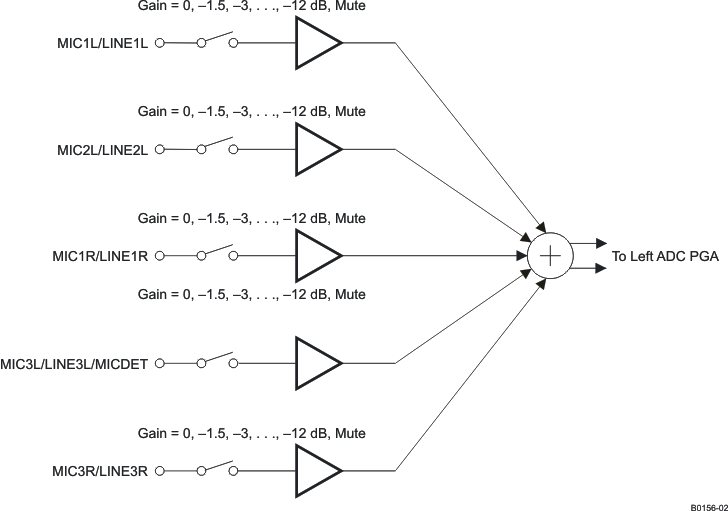 Figure 21. Left-Channel, Single-Ended Analog Input Mixing Configuration
10.3.5 Analog Fully Differential Line Output Drivers
The TLV320AIC3105 has two fully differential line output drivers, each capable of driving a 10-kΩ differential load. The output stage design leading to the fully differential line output drivers is shown in Figure 22 and Figure 23. This design includes extensive capability to adjust signal levels independently before any mixing occurs, beyond that already provided by the PGA gain and the DAC digital volume control.
The LINE2L/R signals refer to the signals that travel through the analog input bypass path to the output stage. The PGA_L/R signals refer to the outputs of the ADC PGA stages that are similarly passed around the ADC to the output stage. Note that because both left- and right-channel signals are routed to all output drivers, a mono mix of any of the stereo signals can easily be obtained by setting the volume controls of both left- and right-channel signals to –6 dB and mixing them. Undesired signals can also be disconnected from the mix as well through register control.
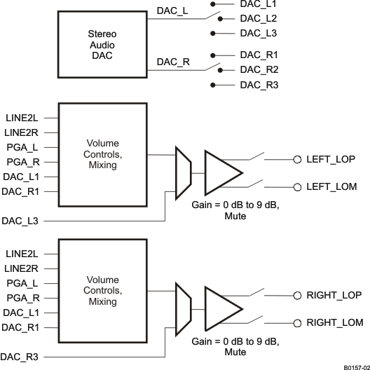 Figure 22. Architecture of the Output Stage Leading to the Fully Differential Line Output Drivers
The DAC_L/R signals are the outputs of the stereo audio DAC, which can be steered by register control based on the requirements of the system. If mixing of the DAC audio with other signals is not required, and the DAC output is only needed at the stereo line outputs, then it is recommended to use the routing through path DAC_L3/R3 to the fully differential stereo line outputs. This results not only in higher quality output performance, but also in lower-power operation, because the analog volume controls and mixing blocks ahead of these drivers can be powered down.
If instead the DAC analog output must be routed to multiple output drivers simultaneously (such as to LEFT_LOP/M and RIGHT_LOP/M) or must be mixed with other analog signals, then the DAC outputs should be switched through the DAC_L1/R1 path. This option provides the maximum flexibility for routing of the DAC analog signals to the output drivers
The TLV320AIC3105 includes an output level control on each output driver with limited gain adjustment from 0 dB to 9 dB. The output driver circuitry in this device are designed to provide a low distortion output while playing full-scale stereo DAC signals at a 0-dB gain setting. However, a higher amplitude output can be obtained at the cost of increased signal distortion at the output. This output level control allows the user to make this tradeoff based on the requirements of the end equipment. Note that this output level control is not intended to be used as a standard output volume control. It is expected to be used only sparingly for level setting, i.e., adjustment of the fullscale output range of the device.
Each differential line output driver can be powered down independently of the others when it is not needed in the system. When placed into power down through register programming, the driver output pins are placed into a high-impedance state.
10.3.6 Analog High-Power Output Drivers
The TLV320AIC3105 includes four high-power output drivers with extensive flexibility in their usage. These output drivers are individually capable of driving 30 mW each into a 16-Ω load in single-ended configuration, and they can be used in pairs connected in bridge-terminated load (BTL) configuration between two driver outputs.
The high-power output drivers can be configured in a variety of ways, including:
- Driving up to two fully differential output signals
- Driving up to four single-ended output signals
- Driving two single-ended output signals, with one or two of the remaining drivers driving a fixed VCM level, for a pseudo differential stereo output
The output stage architecture leading to the high-power output drivers is shown in Figure 24, with the volume control and mixing blocks being effectively identical to that shown in Figure 23. Note that each of these drivers have a output level control block like those included with the line output drivers, allowing gain adjustment up to 9 dB on the output signal. As in the previous case, this output level adjustment is not intended to be used as a standard volume control, but instead is included for additional fullscale output signal level control.
Two of the output drivers, HPROUT and HPLOUT, include a direct connection path for the stereo DAC outputs to be passed directly to the output drivers and bypass the analog volume controls and mixing networks, using the DAC_L2/R2 path. As in the line output case, this functionality provides the highest quality DAC playback performance with reduced power dissipation, but can only be utilized if the DAC output does not need to route to multiple output drivers simultaneously, and if mixing of the DAC output with other analog signals is not needed.
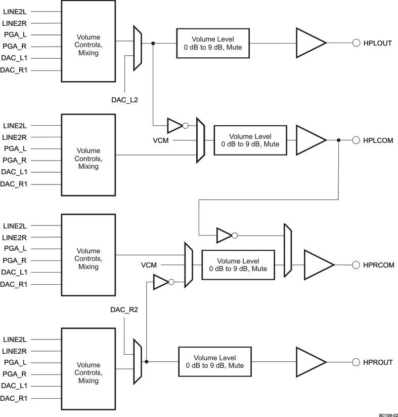 Figure 24. Architecture of the Output Stage Leading to the High-Power Output Drivers
The high-power output drivers include additional circuitry to avoid artifacts on the audio output during power-on and power-off transient conditions. The user should first program the type of output configuration being used in page 0, register 14 to allow the device to select the optimal power-up scheme to avoid output artifacts. The power-up delay time for the high-power output drivers is also programmable over a wide range of time delays, from instantaneous up to 4 s, using page 0, register 42.
When these output drivers are powered down, they can be placed into a variety of output conditions based on register programming. If lowest-power operation is desired, then the outputs can be placed into a high-impedance state, and all power to the output stage is removed. However, this generally results in the output nodes drifting to rest near the upper or lower analog supply, due to small leakage currents at the pins. This then results in a longer delay requirement to avoid output artifacts during driver power on. In order to reduce this required power-on delay, the TLV320AIC3105 includes an option for the output pins of the drivers to be weakly driven to the VCM level they would normally rest at when powered with no signal applied. This output VCM level is determined by an internal bandgap voltage reference, and thus results in extra power dissipation when the drivers are in power down. However, this option provides the fastest method for transitioning the drivers from power down to full-power operation without any output artifact introduced.
The device includes a further option that falls between the other two—although it requires less power drawn while the output drivers are in power down, it also takes a slightly longer delay to power up without artifact than if the bandgap reference is kept alive. In this alternate mode, the powered-down output driver pin is weakly driven to a voltage of approximately half the DRVDD1/2 supply level using an internal voltage divider. This voltage does not match the actual VCM of a fully powered driver, but due to the output voltage being close to its final value, a much shorter power-up delay time setting can be used and still avoid any audible output artifacts. These output voltage options are controlled in page 0, register 42.
The high-power output drivers can also be programmed to power up first with the output level (gain) control in a highly attenuated state; then the output driver automatically reduces the output attenuation slowly to reach the programmed output gain. This capability is enabled by default but can be disabled in page 0, register 40.
10.3.7 Input Impedance and VCM Control
The TLV320AIC3105 includes several programmable settings to control analog input pins, particularly when they are not selected for connection to an ADC PGA. The default option allows unselected inputs to be put into a high-impedance state, such that the input impedance seen looking into the device is extremely high. Note, however, that the pins on the device do include protection diode circuits connected to AVDD and AVSS. Thus, if any voltage is driven onto a pin approximately one diode drop (~0.6 V) above AVDD or one diode drop below AVSS, these protection diodes begin conducting current, resulting in an effective impedance that no longer appears as a high-impedance state.
Another programmable option for unselected analog inputs is to weakly hold them at the common-mode input voltage of the ADC PGA (which is determined by an internal bandgap voltage reference). This is useful to keep the ac-coupling capacitors connected to analog inputs biased up at a normal dc level, thus avoiding the need for them to charge up suddenly when the input is changed from being unselected to selected for connection to an ADC PGA. This option is controlled in page 0, registers 20 and 23. The user should ensure this option is disabled when an input is selected for connection to an ADC PGA or selected for the analog input bypass path, because it can corrupt the recorded input signal if left operational when an input is selected.
In most cases, the analog input pins on the TLV320AIC3105 should be ac-coupled to analog input sources, the only exception to this generally being if an ADC is being used for dc voltage measurement. The ac-coupling capacitor causes a high-pass filter pole to be inserted into the analog signal path, so the size of the capacitor must be chosen to move that filter pole sufficiently low in frequency to cause minimal effect on the processed analog signal. The input impedance of the analog inputs when selected for connection to an ADC PGA varies with the setting of the input level control, starting at approximately 20 kΩ with an input level control setting of 0 dB, and increasing to approximately 80 kΩ when the input level control is set at –12 dB. For example, using a 0.1-µF ac-coupling capacitor at an analog input results in a high-pass filter pole of 80 Hz when the 0-dB input level control setting is selected.
10.3.8 MICBIAS Generation
The TLV320AIC3105 includes a programmable microphone bias output voltage (MICBIAS), capable of providing output voltages of 2 V or 2.5 V (both derived from the on-chip bandgap voltage) with 4-mA output current drive. In addition, the MICBIAS may be programmed to be switched to AVDD directly through an on-chip switch, or it can be powered down completely when not needed, for power savings. This function is controlled by register programming in page 0, register 25.
10.3.9 Short-Circuit Output Protection
The TLV320AIC3105 includes programmable short-circuit protection for the high-power output drivers, for maximum flexibility in a given application. By default, if these output drivers are shorted, they automatically limit the maximum amount of current that can be sourced to or sunk from a load, thereby protecting the device from an overcurrent condition. In this mode, the user can read page 0, register 95 to determine whether the part is in short-circuit protection or not, and then decide whether to program the device to power down the output drivers. However, the device includes further capability to power down an output driver automatically whenever it goes into short-circuit protection, without requiring intervention from the user. In this case, the output driver stays in a power-down condition until the user specifically programs it to power down and then power back up again, to clear the short-circuit flag.
10.3.10 Jack and Headset Detection
The TLV320AIC3105 includes extensive capability to monitor a headphone, microphone, or headset jack, determine if a plug has been inserted into the jack, and then determine what type of headset/headphone is wired to the plug. Figure 25 shows one configuration of the device that enables detection and determination of headset type when a pseudo-differential (capless) stereo headphone output configuration is used. The registers used for this function are page 0, registers 14, 96, 97, and 13. The type of headset detected can be read back from page 0, register 13. Note that for best results, it is recommended to select a MICBIAS value as high as possible, and to program the output driver common-mode level at a 1.35-V or 1.5-V level.
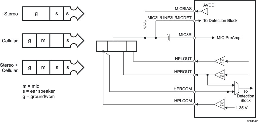 Figure 25. Configuration of Device for Jack Detection Using a
 Pseudo-Differential (Capless) Headphone Output Connection
A modified output configuration used when the output drivers are ac-coupled is shown in Figure 26. Note that in this mode, the device cannot accurately determine if the inserted headphone is a mono or stereo headphone.
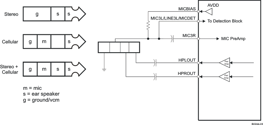 Figure 26. Configuration of Device for Jack Detection Using
 an AC-Coupled Stereo Headphone Output Connection
An output configuration for the case of the outputs driving fully differential stereo headphones is shown in Figure 27. In this mode, there is a requirement on the jack side that either HPLCOM or HPLOUT get shorted to ground if the plug is removed, which can be implemented using a spring terminal in a jack. For this mode to function properly, short-circuit detection should be enabled and configured to power down the drivers if a short-circuit is detected. The registers that control this functionality are in page 0, register 38, bits D2–D1.
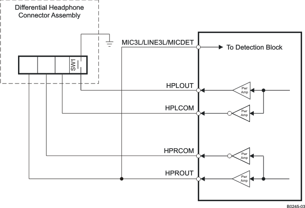 Figure 27. Configuration of Device for Jack Detection Using a
 Fully Differential Stereo Headphone Output Connection
10.4 Device Functional Modes
10.4.1 Bypass Path Mode
The TLV320AIC3105 is a versatile device designed for low-power applications. In some cases, only a few features of the device are required. For these applications, the unused stages of the device must be powered down to save power and an alternate route should be used. This is called a bypass path. The bypass path modes let the device to save power by turning off unused stages, like ADC, DAC and PGA.
10.4.1.1 Analog Input Bypass Path Functionality
The TLV320AIC3105 includes the additional ability to route some analog input signals past the integrated data converters, for mixing with other analog signals and then direct connection to the output drivers. This capability is useful in a cell phone, for example, when a separate FM radio device provides a stereo analog output signal that needs to be routed to headphones. The TLV320AIC3105 supports this in a low-power mode by providing a direct analog path through the device to the output drivers, while all ADCs and DACs can be completely powered down to save power.
When programmed correctly, the device can pass the LINE2L and LINE2R signals directly to the output stage.
10.4.1.2 ADC PGA Signal Bypass Path Functionality
In addition to the input bypass path described above, the TLV320AIC3105 also includes the ability to route the ADC PGA output signals past the ADC, for mixing with other analog signals and then direct connection to the output drivers. These bypass functions are described in more detail in the sections on output mixing and output driver configurations.
10.4.1.3 Passive Analog Bypass During Power Down
Programming the TLV320AIC3105 to passive analog bypass occurs by configuring the output stage switches for passthrough. This is done by opening switches SW-L0, SW-R0 and closing either SW-L1 or SW-L2 and SW-R1 or SW-R2. See Figure 28. Programming this mode is done by writing to page 0, register 108.
Connecting the MIC1L/LINE1L input signal to LEFT_LOP is done by closing SW-L1 and opening SW-L0; this action is done by writing a 1 to page 0, register 108, bit D0. Connecting the MIC2L/LINE2L input signal to LEFT_LOP is done by closing SW-L2 and opening SW-L0; this action is done by writing a 1 to page 0, register 108, bit D2.
Connecting the MIC1R/LINE1R input signal to RIGHT_LOP is done by closing SW-R1 and opening SW-R0; this action is done by writing a 1 to page 0, register 108, bit D4. Connecting the MIC2R/LINE2R input signal to RIGHT_LOP is done by closing SW-R2 and opening SW-R0; this action is done by writing a 1 to page 0, register 108, bit D6. A diagram of the passive analog bypass mode configuration can be seen in Figure 28.
In general, connecting two switches to the same output pin should be avoided, as this error shorts two input signals together, and would likely cause distortion of the signal as the two signals are in contention. Poor frequency response would also likely occur.
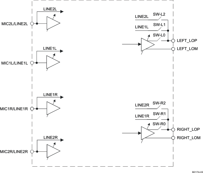 Figure 28. Passive Analog Bypass Mode Configuration
10.4.2 Digital Audio Processing for Record Path
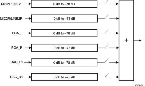
In applications where record only is selected, and DAC is powered down, the playback path signal processing blocks can be used in the ADC record path. These filtering blocks can support high-pass, low-pass, band-pass or notch filtering. In this mode, the record only path has switches SW-D1 through SW-D4 closed, and reroutes the ADC output data through the digital signal processing blocks. Because the DAC digital signal processing blocks are being re-used, naturally the addresses of these digital filter coefficients are the same as for the DAC digital processing and are located on page 1, registers 1–52. This record only mode is enabled by powering down both DACs by writing to page 0, register 37, bits D7–D6 (D7 = D6 = 0). Next, enable the digital filter pathway for the ADC by writing a 1 to page 0, register 107, bit D3. (Note, this pathway is only enabled if both DACs are powered down.) This record only path can be seen in Figure 29.
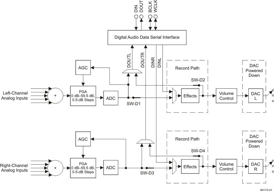 Figure 29. Record-Only Mode With Digital Processing Path Enabled
10.5 Programming
10.5.1 I2C Control Interface
The TLV320AIC3105 supports the I2C control protocol using 7-bit addressing and is capable of both standard and fast modes. For I2C fast mode, note that the minimum timing for each of tHD-STA, tSU-STA, and tSU-STO is 0.9 s, as seen in Figure 30. The TLV320AIC3105 responds to the I2C address of 001 1000. I2C is a two-wire, open-drain interface supporting multiple devices and masters on a single bus. Devices on the I2C bus only drive the bus lines LOW by connecting them to ground; they never drive the bus lines HIGH. Instead, the bus wires are pulled HIGH by pullup resistors, so the bus wires are HIGH when no device is driving them LOW. This way, two devices cannot conflict; if two devices drive the bus simultaneously, there is no driver contention.
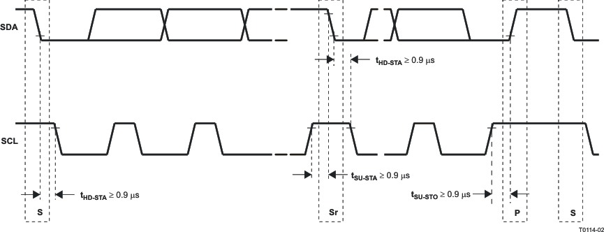 Figure 30. I2C Interface Timing
Communication on the I2C bus always takes place between two devices, one acting as the master and the other acting as the slave. Both masters and slaves can read and write, but slaves can only do so under the direction of the master. Some I2C devices can act as masters or slaves, but the TLV320AIC3105 can only act as a slave device.
An I2C bus consists of two lines, SDA and SCL. SDA carries data; SCL provides the clock. All data is transmitted across the I2C bus in groups of eight bits. To send a bit on the I2C bus, the SDA line is driven to the appropriate level while SCL is LOW (a LOW on SDA indicates the bit is zero; a HIGH indicates the bit is one). Once the SDA line has settled, the SCL line is brought HIGH, then LOW. This pulse on SCL clocks the SDA bit into the receivers shift register.
The I2C bus is bidirectional: the SDA line is used both for transmitting and receiving data. When a master reads from a slave, the slave drives the data line; when a master sends to a slave, the master drives the data line. Under normal circumstances the master drives the clock line.
Most of the time the bus is idle, no communication is taking place, and both lines are HIGH. When communication is taking place, the bus is active. Only master devices can start a communication. They do this by causing a START condition on the bus. Normally, the data line is only allowed to change state while the clock line is LOW. If the data line changes state while the clock line is HIGH, it is either a START condition or its counterpart, a STOP condition. A START condition is when the clock line is HIGH and the data line goes from HIGH to LOW. A STOP condition is when the clock line is HIGH and the data line goes from LOW to HIGH.
After the master issues a START condition, it sends a byte that indicates which slave device it wants to communicate with. This byte is called the address byte. Each device on an I2C bus has a unique 7-bit address to which it responds. (Slaves can also have 10-bit addresses; see the I2C specification for details.) The master sends an address in the address byte, together with a bit that indicates whether it wishes to read from or write to the slave device.
Every byte transmitted on the I2C bus, whether it is address or data, is acknowledged with an acknowledge bit. When a master has finished sending a byte (eight data bits) to a slave, it stops driving SDA and waits for the slave to acknowledge the byte. The slave acknowledges the byte by pulling SDA LOW. The master then sends a clock pulse to clock the acknowledge bit. Similarly, when a master has finished reading a byte, it pulls SDA LOW to acknowledge this to the slave. It then sends a clock pulse to clock the bit.
A not-acknowledge is performed by simply leaving SDA HIGH during an acknowledge cycle. If a device is not present on the bus, and the master attempts to address it, it receives a not-acknowledge because no device is present at that address to pull the line LOW.
When a master has finished communicating with a slave, it may issue a STOP condition. When a STOP condition is issued, the bus becomes idle again. A master may also issue another START condition. When a START condition is issued while the bus is active, it is called a repeated START condition.
The TLV320AIC3105 also responds to and acknowledges a General Call, which consists of the master issuing a command with a slave address byte of 00H.
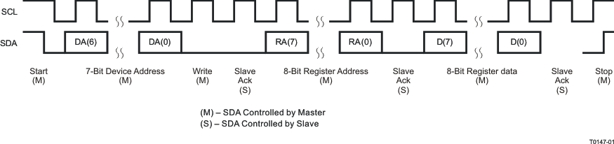 Figure 31. I2C Write
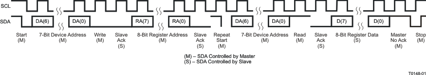 Figure 32. I2C Read
In the case of an I2C register write, if the master does not issue a STOP condition, then the device enters auto-increment mode. So in the next eight clocks, the data on SDA is treated as data for the next incremental register.
Similarly, in the case of an I2C register read, after the device has sent out the 8-bit data from the addressed register, if the master issues an acknowledge, the slave takes over control of SDA bus and transmit for the next 8 clocks the data of the next incremental register.
10.5.1.1 I2C Bus Debug in a Glitched System
Occasionally, some systems may encounter noise or glitches on the I2C bus. In the unlikely event that this affects bus performance, then it can be useful to use the I2C Debug register. This feature terminates the I2C bus error allowing this I2C device and system to resume communications. The I2C bus error detector is enabled by default. The TLV320AIC3105 I2C error detector status can be read from page 0, register 107, bit D0. If desired, the detector can be disabled by writing to page 0, register 107, bit D2.
10.5.2 Register Map Structure
Audio data is transferred between the host processor and the TLV320AIC3105 via the digital audio data serial interface, or audio bus. The audio bus of the TLV320AIC3105 can be configured for left- or right-justified, I2S, DSP, or TDM modes of operation, where communication with standard telephony PCM interfaces is supported within the TDM mode. These modes are all MSB-first, with data width programmable as 16, 20, 24, or 32 bits. In addition, the word clock (WCLK) and bit clock (BCLK) can be independently configured in either Master or Slave mode, for flexible connectivity to a wide variety of processors.
The word clock (WCLK) is used to define the beginning of a frame, and may be programmed as either a pulse or a square-wave signal. The frequency of this clock corresponds to the maximum of the selected ADC and DAC sampling frequencies.
The bit clock (BCLK) is used to clock in and out the digital audio data across the serial bus. When in Master mode, this signal can be programmed in two further modes: continuous transfer mode, and 256-clock mode. In continuous transfer mode, only the minimal number of bit clocks needed to transfer the audio data are generated, so in general the number of bit clocks per frame is two times the data width. For example, if data width is chosen as 16 bits, then 32 bit clocks are generated per frame. If the bit clock signal in master mode is to be used by a PLL in another device, it is recommended that the 16-bit or 32-bit data width selections be used. These cases result in a low jitter bit clock signal being generated, having frequencies of 32 × fS or 64 × fS. In the cases of 20-bit and 24-bt data width in master mode, the bit clocks generated in each frame are not all of equal period, due to the device not having a clean 40 × fS or 48 × fS clock signal readily available. The average frequency of the bit clock signal is still accurate in these cases (being 40 × fS or 48 × fS), but the resulting clock signal has higher jitter than in the 16-bit and 32-bit cases.
In 256-clock mode, a constant 256 bit clocks per frame are generated, independent of the data width chosen. The TLV320AIC3105 further includes programmability to place the DOUT line in the high-impedance state during all bit clocks when valid data is not being sent. By combining this capability with the ability to program at what bit clock in a frame the audio data begins, time-division multiplexing (TDM) can be accomplished, resulting in multiple codecs able to use a single audio serial data bus.
When the audio serial data bus is powered down while configured in master mode, the pins associated with the interface are put into a high-impedance state.
10.6 Register Maps
10.6.1 Control Registers
The control registers for the TLV320AIC3105 are described in detail below. All registers are 8 bits in width, with D7 referring to the most-significant bit of each register, and D0 referring to the least-significant bit.
Table 5. Page 0/Register 0: Page Select Register
| BIT(1) | READ/ WRITE | RESET VALUE | DESCRIPTION |
|---|---|---|---|
| D7–D1 | X | 0000 000 | Reserved, write only zeros to these register bits |
| D0 | R/W | 0 | Page Select Bit Writing zero to this bit sets page 0 as the active page for following register accesses. Writing a one to this bit sets page 1 as the active page for following register accesses. It is recommended that the user read this register bit back after each write, to ensure that the proper page is being accessed for future register read/writes. |
Table 6. Page 0/Register 1: Software Reset Register
| BIT | READ/ WRITE | RESET VALUE | DESCRIPTION |
|---|---|---|---|
| D7 | W | 0 | Software Reset Bit 0 : Don’t care 1 : Self clearing software reset |
| D6–D0 | W | 000 0000 | Reserved; don’t write |
Table 7. Page 0/Register 2: Codec Sample Rate Select Register
| BIT | READ/ WRITE | RESET VALUE | DESCRIPTION |
|---|---|---|---|
| D7–D4 | R/W | 0000 | ADC Sample Rate Select 0000: ADC fS = fS(ref)/1 0001: ADC fS = fS(ref)/1.5 0010: ADC fS = fS(ref)/2 0011: ADC fS = fS(ref)/2.5 0100: ADC fS = fS(ref)/3 0101: ADC fS = fS(ref)/3.5 0110: ADC fS = fS(ref)/4 0111: ADC fS = fS(ref)/4.5 1000: ADC fS = fS(ref)/5 1001: ADC fS = fS(ref)/5.5 1010: ADC fS = fS(ref)/6 1011–1111: Reserved, do not write these sequences. |
| D3–D0 | R/W | 0000 | DAC Sample Rate Select 0000: DAC fS = fS(ref)/1 0001: DAC fS = fS(ref)/1.5 0010: DAC fS = fS(ref)/2 0011: DAC fS = fS(ref)/2.5 0100: DAC fS = fS(ref)/3 0101: DAC fS = fS(ref)/3.5 0110: DAC fS = fS(ref)/4 0111: DAC fS = fS(ref)/4.5 1000: DAC fS = fS(ref)/5 1001: DAC fS = fS(ref)/5.5 1010: DAC fS = fS(ref)/6 1011–1111 : Reserved, do not write these sequences. |
NOTE
In the TLV320AIC3105, for page 0, register 2, the ADC fS must be set equal to the DAC fS. This is done by setting the value of bits D7–D4 equal to that of bits D3–D0.
Table 8. Page 0/Register 3: PLL Programming Register A
| BIT | READ/ WRITE | RESET VALUE | DESCRIPTION |
|---|---|---|---|
| D7 | R/W | 0 | PLL Control Bit 0: PLL is disabled 1: PLL is enabled |
| D6–D3 | R/W | 0010 | PLL Q Value 0000: Q = 16 0001: Q = 17 0010: Q = 2 0011: Q = 3 0100: Q = 4 … 1110: Q = 14 1111: Q = 15 |
| D2–D1 | R/W | 000 | PLL P Value 000: P = 8 001: P = 1 010: P = 2 011: P = 3 100: P = 4 101: P = 5 110: P = 6 111: P = 7 |
Table 9. Page 0/Register 4: PLL Programming Register B
| BIT | READ/ WRITE | RESET VALUE | DESCRIPTION |
|---|---|---|---|
| D7–D2 | R/W | 0000 01 | PLL J Value 0000 00: Reserved; do not write this sequence. 0000 01: J = 1 0000 10: J = 2 0000 11: J = 3 … 1111 10: J = 62 1111 11: J = 63 |
| D1–D0 | R/W | 00 | Reserved. Write only zeros to these bits. |
Table 10. Page 0/Register 5: PLL Programming Register C (1)
| BIT | READ/ WRITE | RESET VALUE | DESCRIPTION |
|---|---|---|---|
| D7–D0 | R/W | 0000 0000 | PLL D value – Eight most significant bits of a 14-bit unsigned integer valid values for D are from zero to 9999, represented by a 14-bit integer located in Page-0/Reg-5–Reg-6. Values should not be written into these registers that would result in a D value outside the valid range. |
Table 11. Page 0/Register 6: PLL Programming Register D
| BIT | READ/ WRITE | RESET VALUE | DESCRIPTION |
|---|---|---|---|
| D7–D2 | R/W | 0000 00 | PLL D value – Six least significant bits of a 14-bit unsigned integer valid values for D are from zero to 9999, represented by a 14-bit integer located in Page-0/Reg-5–Reg-6. Values should not be written into these registers that would result in a D value outside the valid range. |
| D1–D0 | R | 00 | Reserved. Write only zeros to these bits. |
Table 12. Page 0/Register 7: Codec Datapath Setup Register
| BIT | READ/ WRITE | RESET VALUE | DESCRIPTION |
|---|---|---|---|
| D7 | R/W | 0 | fS(ref) Setting This register setting controls timers related to the AGC time constants. 0: fS(ref) = 48 kHz 1: fS(ref) = 44.1 kHz |
| D6 | R/W | 0 | ADC Dual-Rate Control 0: ADC dual-rate mode is disabled. 1: ADC dual-rate mode is enabled. Note: ADC dual-rate mode must match DAC dual-rate mode. |
| D5 | R/W | 0 | DAC Dual-Rate Control 0: DAC dual-rate mode is disabled. 1: DAC dual-rate mode is enabled. |
| D4–D3 | R/W | 00 | Left-DAC Data Path Control 00: Left-DAC data path is off (muted). 01: Left-DAC data path plays left-channel input data. 10: Left-DAC data path plays right channel input data. 11: Left-DAC data path plays mono mix of left- and right-channel input data. |
| D2–D1 | R/W | 00 | Right DAC Datapath Control 00: Right DAC datapath is off (muted). 01: Right DAC datapath plays right-channel input data. 10: Right DAC datapath plays left-channel input data. 11: Right DAC datapath plays mono mix of left- and right-channel input data. |
| D0 | R/W | 0 | Reserved. Only write zero to this register. |
Table 13. Page 0/Register 8: Audio Serial Data Interface Control Register A
| BIT | READ/ WRITE | RESET VALUE | DESCRIPTION | |
|---|---|---|---|---|
| D7 | R/W | 0 | Bit Clock Directional Control 0: BCLK is an input (slave mode) 1: BCLK is an output (master mode) |
|
| D6 | R/W | 0 | Word Clock Directional Control 0: WCLK is an input (slave mode) 1: WCLK is an output (master mode) |
|
| D5 | R/W | 0 | Serial Output Data Driver (DOUT) 3-State Control | |
| 0: | Do not place DOUT in high-impedance state when valid data is not being sent. | |||
| 1: | Place DOUT in high-impedance state when valid data is not being sent. | |||
| D4 | R/W | 0 | Bit/ Word Clock Drive Control 0: BCLK/WCLK does not continue to be transmitted when running in master mode if codec is powered down. 1: BCLK/WCLK continues to be transmitted when running in master mode, even if codec is powered down. |
|
| D3 | R/W | 0 | Reserved. Do not write to this register bit. | |
| D2 | R/W | 0 | 3-D Effect Control 0: Disable 3-D digital effect processing 1: Enable 3-D digital effect processing |
|
| D1–D0 | R/W | 00 | Reserved. Write only 00 to these bits. | |
Table 14. Page 0/Register 9: Audio Serial Data Interface Control Register B
| BIT | READ/ WRITE | RESET VALUE | DESCRIPTION |
|---|---|---|---|
| D7–D6 | R/W | 00 | Audio Serial Data Interface Transfer Mode 00: Serial data bus uses I2S mode 01: Serial data bus uses DSP mode 10: Serial data bus uses right-justified mode 11: Serial data bus uses left-justified mode |
| D5–D4 | R/W | 00 | Audio Serial Data Word Length Control 00: Audio data word length = 16 bits 01: Audio data word length = 20 bits 10: Audio data word length = 24 bits 11: Audio data word length = 32 bits |
| D3 | R/W | 0 | Bit Clock Rate Control This register only has effect when bit clock is programmed as an output 0: Continuous-transfer mode used to determine master mode bit clock rate 1: 256-clock transfer mode used, resulting in 256 bit clocks per frame |
| D2 | R/W | 0 | DAC Re-Sync 0: Don’t Care 1: Re-sync stereo DAC with codec interface if the group delay changes by more than ±DAC (fS/4). |
| D1 | R/W | 0 | ADC Re-Sync 0: Don’t Care 1: Re-sync stereo ADC with codec interface if the group delay changes by more than ±ADC (fS/4). |
| D0 | R/W | Re-Sync Mute Behavior 0: Re-sync is done without soft-muting the channel (ADC/DAC). 1: Re-sync is done by internally soft-muting the channel (ADC/DAC). |
Table 15. Page 0/Register 10: Audio Serial Data Interface Control Register C
| BIT | READ/ WRITE | RESET VALUE | DESCRIPTION |
|---|---|---|---|
| D7–D0 | R/W | 0000 0000 | Audio Serial Data Word Offset Control This register determines where valid data is placed or expected in each frame, by controlling the offset from beginning of the frame where valid data begins. The offset is measured from the rising edge of word clock when in DSP mode. 0000 0000: Data offset = 0 bit clocks 0000 0001: Data offset = 1 bit clock 0000 0010: Data offset = 2 bit clocks … Note: In continuous transfer mode the maximum offset is 17 for I2S/LJF/RJF modes and 16 for DSP mode. In 256-clock mode, the maximum offset is 242 for I2S/LJF/RJF and 241 for DSP modes. 1111 1110: Data offset = 254 bit clocks 1111 1111: Data offset = 255 bit clocks |
Table 16. Page 0/Register 11: Audio Codec Overflow Flag Register
| BIT | READ/ WRITE | RESET VALUE | DESCRIPTION |
|---|---|---|---|
| D7 | R | 0 | Left-ADC Overflow Flag This is a sticky bit, which stays set if an overflow occurs, even if the overflow condition is removed. The register bit reset to 0 after it is read. 0: No overflow has occurred. 1: An overflow has occurred. |
| D6 | R | 0 | Right ADC Overflow Flag This is a sticky bit, which stays set if an overflow occurs, even if the overflow condition is removed. The register bit reset to 0 after it is read. 0: No overflow has occurred. 1: An overflow has occurred. |
| D5 | R | 0 | Left-DAC Overflow Flag This is a sticky bit, which stays set if an overflow occurs, even if the overflow condition is removed. The register bit reset to 0 after it is read. 0: No overflow has occurred. 1: An overflow has occurred. |
| D4 | R | 0 | Right DAC Overflow Flag This is a sticky bit, which stays set if an overflow occurs, even if the overflow condition is removed. The register bit reset to 0 after it is read. 0: No overflow has occurred. 1: An overflow has occurred. |
| D3–D0 | R/W | 0001 | PLL R Value 0000: R = 16 0001: R = 1 0010: R = 2 0011: R = 3 0100: R = 4 … 1110: R = 14 1111: R = 15 |
Table 17. Page 0/Register 12: Audio Codec Digital Filter Control Register
| BIT | READ/ WRITE | RESET VALUE | DESCRIPTION |
|---|---|---|---|
| D7–D6 | R/W | 00 | Left-ADC High-Pass Filter Control 00: Left-ADC high-pass filter disabled 01: Left-ADC high-pass filter –3-dB frequency = 0.0045 × ADC fS 10: Left-ADC high-pass filter –3-dB frequency = 0.0125 × ADC fS 11: Left-ADC high-pass filter –3-dB frequency = 0.025 × ADC fS |
| D5–R4 | R/W | 00 | Right ADC High-Pass Filter Control 00: Right ADC high-pass filter disabled 01: Right ADC high-pass filter –3-dB frequency = 0.0045 × ADC fS 10: Right ADC high-pass filter –3-dB frequency = 0.0125 × ADC fS 11: Right ADC high-pass filter –3-dB frequency = 0.025 × ADC fS |
| D3 | R/W | 0 | Left-DAC Digital Effects Filter Control 0: Left-DAC digital effects filter disabled (bypassed) 1: Left-DAC digital effects filter enabled |
| D2 | R/W | 0 | Left-DAC De-Emphasis Filter Control 0: Left-DAC de-emphasis filter disabled (bypassed) 1: Left-DAC de-emphasis filter enabled |
| D1 | R/W | 0 | Right DAC Digital Effects Filter Control 0: Right DAC digital effects filter disabled (bypassed) 1: Right DAC digital effects filter enabled |
| D0 | R/W | 0 | Right DAC De-Emphasis Filter Control 0: Right DAC de-emphasis filter disabled (bypassed) 1: Right DAC de-emphasis filter enabled |
Table 18. Page 0/Register 13: Reserved
| BIT | READ/ WRITE | RESET VALUE | DESCRIPTION |
|---|---|---|---|
| D7–D0 | R/W | 0000 0000 | Reserved. Write only 0000 0000 to these bits. |
Table 19. Page 0/Register 14: Headset/Button Press Detection Register B
| BIT | READ/ WRITE | RESET VALUE | DESCRIPTION |
|---|---|---|---|
| D7 | R/W | 0 | Driver Capacitive Coupling 0: Programs high-power outputs for capless driver configuration 1: Programs high-power outputs for ac-coupled driver configuration |
| D6 | R/W | 0 | Stereo Output Driver Configuration A Note: Do not set bits D6 and D3 both high at the same time. 0: A stereo fully differential output configuration is not being used 1: A stereo fully differential output configuration is being used |
| D5 | R | 0 | Reserved. Write only zero to this bit. |
| D4 | R | 0 | Headset Detection Flag 0: A headset has not been detected. 1: A headset has been detected. |
| D3 | R/W | 0 | Stereo Output Driver Configuration B Note: Do not set bits D6 and D3 both high at the same time. 0: A stereo pseudo differential output configuration is not being used. 1: A stereo pseudo differential output configuration is being used. |
| D2–D0 | R | 000 | Reserved. Write only zeros to these bits. |
Table 20. Page 0/Register 15: Left-ADC PGA Gain Control Register
| BIT | READ/ WRITE | RESET VALUE | DESCRIPTION |
|---|---|---|---|
| D7 | R/W | 1 | Left-ADC PGA Mute 0: The left-ADC PGA is not muted 1: The left-ADC PGA is muted |
| D6–D0 | R/W | 000 0000 | Left-ADC PGA Gain Setting 000 0000: Gain = 0 dB 000 0001: Gain = 0.5 dB 000 0010: Gain = 1 dB … 111 0110: Gain = 59 dB 111 0111: Gain = 59.5 dB 111 1000: Gain = 59.5 dB … 111 1111: Gain = 59.5 dB |
Table 21. Page 0/Register 15: Left-ADC PGA Gain Control Register
| BIT | READ/ WRITE | RESET VALUE | DESCRIPTION |
|---|---|---|---|
| D7 | R/W | 1 | Left-ADC PGA Mute 0: The left-ADC PGA is not muted 1: The left-ADC PGA is muted |
| D6–D0 | R/W | 000 0000 | Left-ADC PGA Gain Setting 000 0000: Gain = 0 dB 000 0001: Gain = 0.5 dB 000 0010: Gain = 1 dB … 111 0110: Gain = 59 dB 111 0111: Gain = 59.5 dB 111 1000: Gain = 59.5 dB … 111 1111: Gain = 59.5 dB |
Table 22. Page 0/Register 17: MIC3L/R to Left-ADC Control Register
| BIT | READ/ WRITE | RESET VALUE | DESCRIPTION |
|---|---|---|---|
| D7–D4 | R/W | 1111 | MIC3L Input Level Control for Left-ADC PGA Mix Setting the input level control to a gain below automatically connects MIC3L to the left-ADC PGA mix. 0000: Input level control gain = 0 dB 0001: Input level control gain = –1.5 dB 0010: Input level control gain = –3 dB 0011: Input level control gain = –4.5 dB 0100: Input level control gain = –6 dB 0101: Input level control gain = –7.5 dB 0110: Input level control gain = –9 dB 0111: Input level control gain = –10.5 dB 1000: Input level control gain = –12 dB 1001–1110: Reserved. Do not write these sequences to these register bits. 1111: MIC3L is not connected to the left-ADC PGA. |
| D3–D0 | R/W | 1111 | MIC3R Input Level Control for Left-ADC PGA Mix Setting the input level control to a gain below automatically connects MIC3R to the left-ADC PGA mix. 0000: Input level control gain = 0 dB 0001: Input level control gain = –1.5 dB 0010: Input level control gain = –3 dB 0011: Input level control gain = –4.5 dB 0100: Input level control gain = –6 dB 0101: Input level control gain = –7.5 dB 0110: Input level control gain = –9 dB 0111: Input level control gain = –10.5 dB 1000: Input level control gain = –12 dB 1001–1110: Reserved. Do not write these sequences to these register bits. 1111: MIC3R is not connected to the left-ADC PGA. |
Table 23. Page 0/Register 18: MIC3L/R to Right ADC Control Register
| BIT | READ/ WRITE | RESET VALUE | DESCRIPTION |
|---|---|---|---|
| D7–D4 | R/W | 1111 | MIC3L Input Level Control for Right ADC PGA Mix Setting the input level control to a gain below automatically connects MIC3L to the right-ADC PGA mix. 0000: Input level control gain = 0 dB 0001: Input level control gain = –1.5 dB 0010: Input level control gain = –3 dB 0011: Input level control gain = –4.5 dB 0100: Input level control gain = –6 dB 0101: Input level control gain = –7.5 dB 0110: Input level control gain = –9 dB 0111: Input level control gain = –10.5 dB 1000: Input level control gain = –12 dB 1001–1110: Reserved. Do not write these sequences to these register bits. 1111: MIC3L is not connected to the left-ADC PGA. |
| D3–D0 | R/W | 1111 | MIC3R Input Level Control for Right ADC PGA Mix Setting the input level control to a gain below automatically connects MIC3R to the right-ADC PGA mix. 0000: Input level control gain = 0 dB 0001: Input level control gain = –1.5 dB 0010: Input level control gain = –3 dB 0011: Input level control gain = –4.5 dB 0100: Input level control gain = –6 dB 0101: Input level control gain = –7.5 dB 0110: Input level control gain = –9 dB 0111: Input level control gain = –10.5 dB 1000: Input level control gain = –12 dB 1001–1110: Reserved. Do not write these sequences to these register bits. 1111: MIC3R is not connected to the left-ADC PGA. |
Table 24. Page 0/Register 19: LINE1L to Left-ADC Control Register
| BIT | READ/ WRITE | RESET VALUE | DESCRIPTION |
|---|---|---|---|
| D7 | R/W | 0 | Reserved |
| D6–D3 | R/W | 1111 | LINE1L Input Level Control for Left-ADC PGA Mix Setting the input level control to a gain below automatically connects LINE1L to the left-ADC PGA mix. 0000: Input level control gain = 0 dB 0001: Input level control gain = –1.5 dB 0010: Input level control gain = –3 dB 0011: Input level control gain = –4.5 dB 0100: Input level control gain = –6 dB 0101: Input level control gain = –7.5 dB 0110: Input level control gain = –9 dB 0111: Input level control gain = –10.5 dB 1000: Input level control gain = –12 dB 1001–1110: Reserved. Do not write these sequences to these register bits. 1111: LINE1L is not connected to the left-ADC PGA. |
| D2 | R/W | 0 | Left-ADC Channel Power Control 0: Left-ADC channel is powered down. 1: Left-ADC channel is powered up. |
| D1–D0 | R/W | 00 | Left-ADC PGA Soft-Stepping Control 00: Left-ADC PGA soft-stepping at once per fS 01: Left-ADC PGA soft-stepping at once per two fS 10–11: Left-ADC PGA soft-stepping is disabled. |
Table 25. Page 0/Register 20: LINE2L to Left (1)-ADC Control Register
| BIT | READ/ WRITE | RESET VALUE | DESCRIPTION |
|---|---|---|---|
| D7 | R/W | 0 | Reserved |
| D6–D3 | R/W | 1111 | LINE2L Input Level Control for Left-ADC PGA Mix Setting the input level control to a gain below automatically connects LINE2L to the left-ADC PGA mix. 0000: Input level control gain = 0 dB 0001: Input level control gain = –1.5 dB 0010: Input level control gain = –3 dB 0011: Input level control gain = –4.5 dB 0100: Input level control gain = –6 dB 0101: Input level control gain = –7.5 dB 0110: Input level control gain = –9 dB 0111: Input level control gain = –10.5 dB 1000: Input level control gain = –12 dB 1001–1110: Reserved. Do not write these sequences to these register bits. 1111: LINE2L is not connected to the left-ADC PGA. |
| D2 | R/W | 0 | Left-ADC-Channel Weak Common-Mode Bias Control 0: Left-ADC-channel unselected inputs are not biased weakly to the ADC common-mode voltage. 1: Left-ADC-channel unselected inputs are biased weakly to the ADC common-mode voltage. |
| D1–D0 | R | 00 | Reserved. Write only zeros to these register bits |
Table 26. Page 0/Register 21: LINE1R to Left-ADC Control Register
| BIT | READ/ WRITE | RESET VALUE | DESCRIPTION |
|---|---|---|---|
| D7 | R/W | 0 | Reserved |
| D6–D3 | R/W | 1111 | LINE1R Input Level Control for Left-ADC PGA Mix Setting the input level control to a gain below automatically connects LINE1R to the left-ADC PGA mix. 0000: Input level control gain = 0 dB 0001: Input level control gain = –1.5 dB 0010: Input level control gain = –3 dB 0011: Input level control gain = –4.5 dB 0100: Input level control gain = –6 dB 0101: Input level control gain = –7.5 dB 0110: Input level control gain = –9 dB 0111: Input level control gain = –10.5 dB 1000: Input level control gain = –12 dB 1001–1110: Reserved. Do not write these sequences to these register bits. 1111: LINE1R is not connected to the left-ADC PGA. |
| D2–D0 | R | 000 | Reserved. Write only zeros to these register bits. |
Table 27. Page 0/Register 22: LINE1R to Right ADC Control Register
| BIT | READ/ WRITE | RESET VALUE | DESCRIPTION |
|---|---|---|---|
| D7 | R/W | 0 | Reserved |
| D6–D3 | R/W | 1111 | LINE1R Input Level Control for Right ADC PGA Mix Setting the input level control to a gain below automatically connects LINE1R to the right ADC PGA mix. 0000: Input level control gain = 0 dB 0001: Input level control gain = –1.5 dB 0010: Input level control gain = –3 dB 0011: Input level control gain = –4.5 dB 0100: Input level control gain = –6 dB 0101: Input level control gain = –7.5 dB 0110: Input level control gain = –9 dB 0111: Input level control gain = –10.5 dB 1000: Input level control gain = –12 dB 1001–1110: Reserved. Do not write these sequences to these register bits. 1111: LINE1R is not connected to the left-ADC PGA. |
| D2 | R/W | 0 | Right ADC Channel Power Control 0: Right ADC channel is powered down. 1: Right ADC channel is powered up. |
| D1–D0 | R/W | 00 | Right ADC PGA Soft-Stepping Control 00: Right ADC PGA soft-stepping at once per fS 01: Right ADC PGA soft-stepping at once per two fS 10–11: Right ADC PGA soft-stepping is disabled. |
Table 28. Page 0/Register 23: LINE2R to Right ADC Control Register
| BIT | READ/ WRITE | RESET VALUE | DESCRIPTION |
|---|---|---|---|
| D7 | R/W | 0 | Reserved |
| D6–D3 | R/W | 1111 | LINE2R Input Level Control for Right ADC PGA Mix Setting the input level control to a gain below automatically connects LIN2R to the right ADC PGA mix. 0000: Input level control gain = 0 dB 0001: Input level control gain = –1.5 dB 0010: Input level control gain = –3 dB 0011: Input level control gain = –4.5 dB 0100: Input level control gain = –6 dB 0101: Input level control gain = –7.5 dB 0110: Input level control gain = –9 dB 0111: Input level control gain = –10.5 dB 1000: Input level control gain = –12 dB 1001–1110: Reserved. Do not write these sequences to these register bits. 1111: LINE2R is not connected to the right ADC PGA. |
| D2 | R/W | 0 | Right ADC Channel Weak Common-Mode Bias Control 0: Right ADC channel unselected inputs are not biased weakly to the ADC common-mode voltage. 1: Right ADC channel unselected inputs are biased weakly to the ADC common-mode voltage. |
| D1–D0 | R | 00 | Reserved. Write only zeros to these register bits |
Table 29. Page 0/Register 24: LINE1L to Right ADC Control Register
| BIT | READ/ WRITE | RESET VALUE | DESCRIPTION |
|---|---|---|---|
| D7 | R/W | 0 | Reserved |
| D6–D3 | R/W | 1111 | LINE1L Input Level Control for Right ADC PGA Mix Setting the input level control to a gain below automatically connects LINE1L to the right ADC PGA mix. 0000: Input level control gain = 0 dB 0001: Input level control gain = –1.5 dB 0010: Input level control gain = –3 dB 0011: Input level control gain = –4.5 dB 0100: Input level control gain = –6 dB 0101: Input level control gain = –7.5 dB 0110: Input level control gain = –9 dB 0111: Input level control gain = –10.5 dB 1000: Input level control gain = –12 dB 1001–1110: Reserved. Do not write these sequences to these register bits. 1111: LINE1L is not connected to the right ADC PGA. |
| D2–D0 | R | 000 | Reserved. Write only zeros to these register bits. |
Table 30. Page 0/Register 25: MICBIAS Control Register
| BIT | READ/ WRITE | RESET VALUE | DESCRIPTION |
|---|---|---|---|
| D7–D6 | R/W | 00 | MICBIAS Level Control 00: MICBIAS output is powered down. 01: MICBIAS output is powered to 2 V. 10: MICBIAS output is powered to 2.5 V. 11: MICBIAS output is connected to AVDD |
| D5–D3 | R | 000 | Reserved. Write only zeros to these bits. |
| D2–D0 | R | XXX | Reserved. Write only zeros to these bits. |
Table 31. Page 0/Register 26: Left-AGC Control Register A
| BIT | READ/ WRITE | RESET VALUE | DESCRIPTION |
|---|---|---|---|
| D7 | R/W | 0 | Left-AGC Enable 0: Left AGC is disabled. 1: Left AGC is enabled. |
| D6–D4 | R/W | 000 | Left-AGC Target Level 000: Left-AGC target level = –5.5 dB 001: Left-AGC target level = –8 dB 010: Left-AGC target level = –10 dB 011: Left-AGC target level = –12 dB 100: Left-AGC target level = –14 dB 101: Left-AGC target level = –17 dB 110: Left-AGC target level = –20 dB 111: Left-AGC target level = –24 dB |
| D3–D2 | R/W | 00 | Left-AGC Attack Time These time constants(1) are not accurate when double-rate audio mode is enabled. 00: Left-AGC attack time = 8 ms 01: Left-AGC attack time = 11 ms 10: Left-AGC attack time = 16 ms 11: Left-AGC attack time = 20 ms |
| D1–D0 | R/W | 00 | Left-AGC Decay Time These time constants(1) are not accurate when double-rate audio mode is enabled. 00: Left-AGC decay time = 100 ms 01: Left-AGC decay time = 200 ms 10: Left-AGC decay time = 400 ms 11: Left-AGC decay time = 500 ms |
Table 32. Page 0/Register 27: Left-AGC Control Register B
| BIT | READ/ WRITE | RESET VALUE | DESCRIPTION |
|---|---|---|---|
| D7–D1 | R/W | 1111 111 | Left-AGC Maximum Gain Allowed 0000 000: Maximum gain = 0 dB 0000 001: Maximum gain = 0.5 dB 0000 010: Maximum gain = 1 dB … 1110 110: Maximum gain = 59 dB 1110 111–1111 111: Maximum gain = 59.5 dB |
| D0 | R/W | 0 | Reserved. Write only zero to this bit. |
Table 33. Page 0/Register 28: Left-AGC Control Register C
| BIT | READ/ WRITE | RESET VALUE | DESCRIPTION |
|---|---|---|---|
| D7–D6 | R/W | 00 | Noise Gate Hysteresis Level Control 00: Hysteresis = 1 dB 01: Hysteresis = 2 dB 10: Hysteresis = 3 dB 11: Hysteresis is disabled |
| D5–D1 | R/W | 00 000 | Left-AGC Noise Threshold Control 00 000: Left-AGC noise/silence detection disabled 00 001: Left-AGC noise threshold = –30 dB 00 010: Left-AGC noise threshold = –32 dB 00 011: Left-AGC noise threshold = –34 dB … 11 101: Left-AGC noise threshold = –86 dB 11 110: Left-AGC noise threshold = –88 dB 11 111: Left-AGC noise threshold = –90 dB |
| D0 | R/W | 0 | Left-AGC Clip Stepping Control 0: Left-AGC clip stepping disabled 1: Left-AGC clip stepping enabled |
Table 34. Page 0/Register 29: Right AGC Control Register A
| BIT | READ/ WRITE | RESET VALUE | DESCRIPTION |
|---|---|---|---|
| D7 | R/W | 0 | Right AGC Enable 0: Right AGC is disabled 1: Right AGC is enabled |
| D6–D4 | R/W | 000 | Right AGC Target Level 000: Right AGC target level = –5.5 dB 001: Right AGC target level = –8 dB 010: Right AGC target level = –10 dB 011: Right AGC target level = –12 dB 100: Right AGC target level = –14 dB 101: Right AGC target level = –17 dB 110: Right AGC target level = –20 dB 111: Right AGC target level = –24 dB |
| D3–D2 | R/W | 00 | Right AGC Attack Time These time constants are not accurate when double-rate audio mode is enabled. 00: Right AGC attack time = 8 ms 01: Right AGC attack time = 11 ms 10: Right AGC attack time = 16 ms 11: Right AGC attack time = 20 ms |
| D1–D0 | R/W | 00 | Right AGC Decay Time These time constants are not accurate when double-rate audio mode is enabled. 00: Right AGC decay time = 100 ms 01: Right AGC decay time = 200 ms 10: Right AGC decay time = 400 ms 11: Right AGC decay time = 500 ms |
Table 35. Page 0/Register 30: Right AGC Control Register B
| BIT | READ/ WRITE | RESET VALUE | DESCRIPTION |
|---|---|---|---|
| D7–D1 | R/W | 1111 111 | Right AGC Maximum Gain Allowed 0000 000: Maximum gain = 0 dB 0000 001: Maximum gain = 0.5 dB 0000 010: Maximum gain = 1 dB … 1110 110: Maximum gain = 59 dB 1110 111–111111: Maximum gain = 59.5 dB |
| D0 | R/W | 0 | Reserved. Write only zero to this register bit. |
Table 36. Page 0/Register 31: Right AGC Control Register C
| BIT | READ/ WRITE | RESET VALUE | DESCRIPTION |
|---|---|---|---|
| D7–D6 | R/W | 00 | Noise Gate Hysteresis Level Control 00: Hysteresis = 1 dB 01: Hysteresis = 2 dB 10: Hysteresis = 3 dB 11: Hysteresis is disabled |
| D5–D1 | R/W | 00 000 | Right AGC Noise Threshold Control 00 000: Right AGC Noise/Silence Detection disabled 00 001: Right AGC noise threshold = –30 dB 00 010: Right AGC noise threshold = –32 dB 00 011: Right AGC noise threshold = –34 dB … 11 101: Right AGC noise threshold = –86 dB 11 110: Right AGC noise threshold = –88 dB 11 111: Right AGC noise threshold = –90 dB |
| D0 | R/W | 0 | Right AGC Clip Stepping Control 0: Right AGC clip stepping disabled 1: Right AGC clip stepping enabled |
Table 37. Page 0/Register 32: Left-AGC Gain Register
| BIT | READ/ WRITE | RESET VALUE | DESCRIPTION |
|---|---|---|---|
| D7–D0 | R | 0000 0000 | Left-Channel Gain Applied by AGC Algorithm 1110 1000: Gain = –12.0-dB 1110 1001: Gain = –11.5-dB 1110 1010: Gain = –11.0-dB … 0000 0000: Gain = 0.0-dB 0000 0001: Gain = +0.5-dB … 0111 0110: Gain = +59.0-dB 0111 0111: Gain = +59.5-dB |
Table 38. Page 0/Register 33: Right AGC Gain Register
| BIT | READ/ WRITE | RESET VALUE | DESCRIPTION |
|---|---|---|---|
| D7–D0 | R | 0000 0000 | Right Channel Gain Applied by AGC Algorithm 1110 1000: Gain = –12.0-dB 1110 1001: Gain = –11.5-dB 1110 1010: Gain = –11.0-dB … 0000 0000: Gain = 0.0-dB 0000 0001: Gain = +0.5-dB … 0111 0110: Gain = +59.0-dB 0111 0111: Gain = +59.5-dB |
Table 39. Page 0/Register 34: Left-AGC Noise Gate Debounce Register
| BIT | READ/ WRITE | RESET VALUE | DESCRIPTION |
|---|---|---|---|
| D7–D3 | R/W | 0000 0 | Left-AGC Noise Detection Debounce Control These times(1) are not accurate when double-rate audio mode is enabled. 0000 0: Debounce = 0 ms 0000 1: Debounce = 0.5 ms 0001 0: Debounce = 1 ms 0001 1: Debounce = 2 ms 0010 0: Debounce = 4 ms 0010 1: Debounce = 8 ms 0011 0: Debounce = 16 ms 0011 1: Debounce = 32 ms 0100 0: Debounce = 64 × 1 = 64 ms 0100 1: Debounce = 64 × 2 = 128 ms 0101 0: Debounce = 64 × 3 = 192 ms … 1111 0: Debounce = 64 × 23 = 1472 ms 1111 1: Debounce = 64 × 24 = 1536 ms |
| D2–D0 | R/W | 000 | Left-AGC Signal Detection Debounce Control These times(1) are not accurate when double-rate audio mode is enabled. 000: Debounce = 0 ms 001: Debounce = 0.5 ms 010: Debounce = 1 ms 011: Debounce = 2 ms 100: Debounce = 4 ms 101: Debounce = 8 ms 110: Debounce = 16 ms 111: Debounce = 32 ms |
Table 40. Page 0/Register 35: Right AG Noise Gate Debounce Register
| BIT | READ/ WRITE | RESET VALUE | DESCRIPTION |
|---|---|---|---|
| D7–D3 | R/W | 0000 0 | Right AGC Noise Detection Debounce Control These times(1) are not accurate when double-rate audio mode is enabled. 0000 0: Debounce = 0 ms 0000 1: Debounce = 0.5 ms 0001 0: Debounce = 1 ms 0001 1: Debounce = 2 ms 0010 0: Debounce = 4 ms 0010 1: Debounce = 8 ms 0011 0: Debounce = 16 ms 0011 1: Debounce = 32 ms 0100 0: Debounce = 64 × 1 = 64 ms 0100 1: Debounce = 64 × 2 = 128 ms 0101 0: Debounce = 64 × 3 = 192 ms … 1111 0: Debounce = 64 × 23 = 1472 ms 1111 1: Debounce = 64 × 24 = 1536 ms |
| D2–D0 | R/W | 000 | Right AGC Signal Detection Debounce Control These times(1) are not accurate when double-rate audio mode is enabled. 000: Debounce = 0 ms 001: Debounce = 0.5 ms 010: Debounce = 1 ms 011: Debounce = 2 ms 100: Debounce = 4 ms 101: Debounce = 8 ms 110: Debounce = 16 ms 111: Debounce = 32 ms |
Table 41. Page 0/Register 36: ADC Flag Register
| BIT | READ/ WRITE | RESET VALUE | DESCRIPTION |
|---|---|---|---|
| D7 | R | 0 | Left-ADC PGA Status 0: Applied gain and programmed gain are not the same. 1: Applied gain = programmed gain |
| D6 | R | 0 | Left-ADC Power Status 0: Left ADC is in a power-down state. 1: Left ADC is in a power-up state. |
| D5 | R | 0 | Left-AGC Signal Detection Status 0: Signal power is greater than noise threshold. 1: Signal power is less than noise threshold. |
| D4 | R | 0 | Left-AGC Saturation Flag 0: Left AGC is not saturated. 1: Left-AGC gain applied = maximum allowed gain for left AGC |
| D3 | R | 0 | Right ADC PGA Status 0: Applied gain and programmed gain are not the same. 1: Applied gain = programmed gain |
| D2 | R | 0 | Right ADC Power Status 0: Right ADC is in a power-down state. 1: Right ADC is in a power-up state |
| D1 | R | 0 | Right AGC Signal Detection Status 0: Signal power is greater than noise threshold. 1: Signal power is less than noise threshold. |
| D0 | R | 0 | Right AGC Saturation Flag 0: Right AGC is not saturated 1: Right AGC gain applied = maximum allowed gain for right AGC |
Table 42. Page 0/Register 37: DAC Power and Output Driver Control Register
| BIT | READ/ WRITE | RESET VALUE | DESCRIPTION |
|---|---|---|---|
| D7 | R/W | 0 | Left-DAC Power Control 0: Left DAC is not powered up. 1: Left DAC is powered up. |
| D6 | R/W | 0 | Right DAC Power Control 0: Right DAC is not powered up. 1: Right DAC is powered up. |
| D5–D4 | R/W | 00 | HPLCOM Output Driver Configuration Control 00: HPLCOM configured as differential of HPLOUT 01: HPLCOM configured as constant VCM output 10: HPLCOM configured as independent single-ended output 11: Reserved. Do not write this sequence to these register bits. |
| D3–D0 | R | 000 | Reserved. Write only zeros to these register bits. |
Table 43. Page 0/Register 38: High-Power Output Driver Control Register
| BIT | READ/ WRITE | RESET VALUE | DESCRIPTION | |
|---|---|---|---|---|
| D7–D6 | R | 00 | Reserved. Write only zeros to these register bits. | |
| D5–D3 | R/W | 000 | HPRCOM Output Driver Configuration Control 00 HPRCOM configured as differential of HPROUT 0: 00 HPRCOM configured as constant VCM output 1: 01 HPRCOM configured as independent single-ended output 0: 01 HPRCOM configured as differential of HPLCOM 1: 10 HPRCOM configured as external feedback with HPLCOM as constant VCM output 0: 101–111: Reserved. Do not write these sequences to these register bits. |
|
| D2 | R/W | 0 | Short-Circuit Protection Control 0: Short-circuit protection on all high-power output drivers is disabled. 1: Short-circuit protection on all high-power output drivers is enabled. |
|
| D1 | R/W | 0 | Short-Circuit Protection Mode Control | |
| 0: | If short-circuit protection is enabled, it limits the maximum current to the load. | |||
| 1: | If short-circuit protection is enabled, it powers down the output driver automatically when a short is detected. | |||
| D0 | R | 0 | Reserved. Write only zero to this register bit. | |
Table 44. Page 0/Register 39: Reserved Register
| BIT | READ/ WRITE | RESET VALUE | DESCRIPTION |
|---|---|---|---|
| D7–D0 | R | 0000 0000 | Reserved. Do not write to these bits. |
Table 45. Page 0/Register 40: High-Power Output Stage Control Register
| BIT | READ/ WRITE | RESET VALUE | DESCRIPTION |
|---|---|---|---|
| D7–D6 | R/W | 00 | Output Common-Mode Voltage Control 00: Output common-mode voltage = 1.35 V 01: Output common-mode voltage = 1.5 V 10: Output common-mode voltage = 1.65 V 11: Output common-mode voltage = 1.8 V |
| D5–D4 | R/W | 00 | LINE2L Bypass Path Control 00: LINE2L bypass is disabled 01: LINE2L bypass uses LINE2LP single-ended 1X: Reserved. Do not use. |
| D3–D2 | R/W | 00 | LINE2R Bypass Path Control 00: LINE2R bypass is disabled 01: LINE2R bypass uses LINE2RP single-ended 1X: Reserved. Do not use. |
| D1–D0 | R/W | 00 | Output Volume Control Soft-Stepping 00: Output soft-stepping = one step per fS 01: Output soft-stepping = one step per 2 fS 10: Output soft-stepping disabled 11: Reserved. Do not write this sequence to these register bits. |
Table 46. Page 0/Register 41: DAC Output Switching Control Register
| BIT | READ/ WRITE | RESET VALUE | DESCRIPTION |
|---|---|---|---|
| D7–D6 | R/W | 00 | Left-DAC Output Switching Control 00: Left-DAC output selects DAC_L1 path. 01: Left-DAC output selects DAC_L3 path to left line output driver. 10: Left-DAC output selects DAC_L2 path to left high-power output drivers. 11: Reserved. Do not write this sequence to these register bits. |
| D5–D4 | R/W | 00 | Right DAC Output Switching Control 00: Right DAC output selects DAC_R1 path. 01: Right DAC output selects DAC_R3 path to right line output driver. 10: Right DAC output selects DAC_R2 path to right high-power output drivers. 11: Reserved. Do not write this sequence to these register bits. |
| D3–D2 | R/W | 00 | Reserved. Write only zeros to these bits. |
| D1–D0 | R/W | 00 | DAC Digital Volume Control Functionality 00: Left- and right-DAC channels have independent volume controls. 01: Left-DAC volume follows the right channel control register. 10: Right DAC volume follows the left channel control register. 11: Left- and right-DAC channels have independent volume controls (same as 00). |
Table 47. Page 0/Register 42: Output Driver Pop Reduction Register
| BIT | READ/ WRITE | RESET VALUE | DESCRIPTION |
|---|---|---|---|
| D7–D4 | R/W | 0000 | Output Driver Power-On Delay Control 0000: Driver power-on time = 0 µs 0001: Driver power-on time = 10 µs 0010: Driver power-on time = 100 µs 0011: Driver power-on time = 1 ms 0100: Driver power-on time = 10 ms 0101: Driver power-on time = 50 ms 0110: Driver power-on time = 100 ms 0111: Driver power-on time = 200 ms 1000: Driver power-on time = 400 ms 1001: Driver power-on time = 800 ms 1010: Driver power-on time = 2 s 1011: Driver power-on time = 4 s 1100–1111: Reserved. Do not write these sequences to these register bits. |
| D3–D2 | R/W | 00 | Driver Ramp-Up Step Timing Control 00: Driver ramp-up step time = 0 ms 01: Driver ramp-up step time = 1 ms 10: Driver ramp-up step time = 2 ms 11: Driver ramp-up step time = 4 ms |
| D1 | R/W | 0 | Weak Output Common-Mode Voltage Control 0: Weakly driven output common-mode voltage is generated from resistor divider off the AVDD supply. 1: Weakly driven output common-mode voltage is generated from band-gap reference. |
| D0 | R/W | 0 | Reserved. Write only zero to this register bit. |
Table 48. Page 0/Register 43: Left-DAC Digital Volume Control Register
| BIT | READ/ WRITE | RESET VALUE | DESCRIPTION |
|---|---|---|---|
| D7 | R/W | 1 | Left-DAC Digital Mute 0: The left DAC channel is not muted. 1: The left DAC channel is muted. |
| D6–D0 | R/W | 000 0000 | Left-DAC Digital Volume Control Setting 000 0000: Gain = 0 dB 000 0001: Gain = –0.5 dB 000 0010: Gain = –1 dB … 111 1101: Gain = –62.5 dB 111 1110: Gain = –63 dB 111 1111: Gain = –63.5 dB |
Table 49. Page 0/Register 44: Right DAC Digital Volume Control Register
| BIT | READ/ WRITE | RESET VALUE | DESCRIPTION |
|---|---|---|---|
| D7 | R/W | 1 | Right DAC Digital Mute 0: The right DAC channel is not muted. 1: The right DAC channel is muted. |
| D6–D0 | R/W | 000 0000 | Right DAC Digital Volume Control Setting 000 0000: Gain = 0 dB 000 0001: Gain = –0.5 dB 000 0010: Gain = –1 dB … 111 1101: Gain = –62.5 dB 111 1110: Gain = –63 dB 111 1111: Gain = –63.5 dB |
10.6.2 Output Stage Volume Controls
A basic analog volume control with range from 0 dB to –78 dB and mute is replicated multiple times in the output stage network, connected to each of the analog signals that route to the output stage. In addition, to enable completely independent mixing operations to be performed for each output driver, each analog signal coming into the output stage may have up to seven separate volume controls. These volume controls all have approximately 0.5-dB step programmability over most of the gain range, with steps increasing slightly at the lowest attenuations. Table 50 lists the detailed gain versus programmed setting for this basic volume control.
Table 50. Output Stage Volume Control Settings and Gains
| Gain Setting | Analog Gain (dB) |
Gain Setting | Analog Gain (dB) |
Gain Setting | Analog Gain (dB) |
Gain Setting | Analog Gain (dB) |
|---|---|---|---|---|---|---|---|
| 0 | 0 | 30 | –15 | 60 | –30.1 | 90 | –45.2 |
| 1 | –0.5 | 31 | –15.5 | 61 | –30.6 | 91 | –45.8 |
| 2 | –1 | 32 | –16 | 62 | –31.1 | 92 | –46.2 |
| 3 | –1.5 | 33 | –16.5 | 63 | –31.6 | 93 | –46.7 |
| 4 | –2 | 34 | –17 | 64 | –32.1 | 94 | –47.4 |
| 5 | –2.5 | 35 | –17.5 | 65 | –32.6 | 95 | –47.9 |
| 6 | –3 | 36 | –18 | 66 | –33.1 | 96 | –48.2 |
| 7 | –3.5 | 37 | –18.6 | 67 | –33.6 | 97 | –48.7 |
| 8 | –4 | 38 | –19.1 | 68 | –34.1 | 98 | –49.3 |
| 9 | –4.5 | 39 | –19.6 | 69 | –34.6 | 99 | –50 |
| 10 | –5 | 40 | –20.1 | 70 | –35.1 | 100 | –50.3 |
| 11 | –5.5 | 41 | –20.6 | 71 | –35.7 | 101 | –51 |
| 12 | –6 | 42 | –21.1 | 72 | –36.1 | 102 | –51.4 |
| 13 | –6.5 | 43 | –21.6 | 73 | –36.7 | 103 | –51.8 |
| 14 | –7 | 44 | –22.1 | 74 | –37.1 | 104 | –52.2 |
| 15 | –7.5 | 45 | –22.6 | 75 | –37.7 | 105 | –52.7 |
| 16 | –8 | 46 | –23.1 | 76 | –38.2 | 106 | –53.7 |
| 17 | –8.5 | 47 | –23.6 | 77 | –38.7 | 107 | –54.2 |
| 18 | –9 | 48 | –24.1 | 78 | –39.2 | 108 | –55.3 |
| 19 | –9.5 | 49 | –24.6 | 79 | –39.7 | 109 | –56.7 |
| 20 | –10 | 50 | –25.1 | 80 | –40.2 | 110 | –58.3 |
| 21 | –10.5 | 51 | –25.6 | 81 | –40.7 | 111 | –60.2 |
| 22 | –11 | 52 | –26.1 | 82 | –41.2 | 112 | –62.7 |
| 23 | –11.5 | 53 | –26.6 | 83 | –41.7 | 113 | –64.3 |
| 24 | –12 | 54 | –27.1 | 84 | –42.2 | 114 | –66.2 |
| 25 | –12.5 | 55 | –27.6 | 85 | –42.7 | 115 | –68.7 |
| 26 | –13 | 56 | –28.1 | 86 | –43.2 | 116 | –72.2 |
| 27 | –13.5 | 57 | –28.6 | 87 | –43.8 | 117 | –78.3 |
| 28 | –14 | 58 | –29.1 | 88 | –44.3 | 118–127 | Mute |
| 29 | –14.5 | 59 | –29.6 | 89 | –44.8 |
Table 51. Page 0/Register 45: LINE2L to HPLOUT Volume Control Register
| BIT | READ/ WRITE | RESET VALUE | DESCRIPTION |
|---|---|---|---|
| D7 | R/W | 0 | LINE2L Output Routing Control 0: LINE2L is not routed to HPLOUT 1: LINE2L is routed to HPLOUT |
| D6–D0 | R/W | 000 0000 | LINE2L to HPLOUT Analog Volume Control For 7-bit register setting versus analog gain values, see Table 50. |
Table 52. Page 0/Register 46: PGA_L to HPLOUT Volume Control Register
| BIT | READ/ WRITE | RESET VALUE | DESCRIPTION |
|---|---|---|---|
| D7 | R/W | 0 | PGA_L Output Routing Control 0: PGA_L is not routed to HPLOUT 1: PGA_L is routed to HPLOUT |
| D6–D0 | R/W | 000 0000 | PGA_L to HPLOUT Analog Volume Control For 7-bit register setting versus analog gain values, see Table 50. |
Table 53. Page 0/Register 47: DAC_L1 to HPLOUT Volume Control Register
| BIT | READ/ WRITE | RESET VALUE | DESCRIPTION |
|---|---|---|---|
| D7 | R/W | 0 | DAC_L1 Output Routing Control 0: DAC_L1 is not routed to HPLOUT. 1: DAC_L1 is routed to HPLOUT. |
| D6–D0 | R/W | 000 0000 | DAC_L1 to HPLOUT Analog Volume Control For 7-bit register setting versus analog gain values, see Table 50. |
Table 54. Page 0/Register 48: LINE2R to HPLOUT Volume Control Register
| BIT | READ/ WRITE | RESET VALUE | DESCRIPTION |
|---|---|---|---|
| D7 | R/W | 0 | LINE2R Output Routing Control 0: LINE2R is not routed to HPLOUT 1: LINE2R is routed to HPLOUT |
| D6–D0 | R/W | 000 0000 | LINE2R to HPLOUT Analog Volume Control For 7-bit register setting versus analog gain values, see Table 50. |
Table 55. Page 0/Register 49: PGA_R to HPLOUT Volume Control Register
| BIT | READ/ WRITE | RESET VALUE | DESCRIPTION |
|---|---|---|---|
| D7 | R/W | 0 | PGA_R Output Routing Control 0: PGA_R is not routed to HPLOUT 1: PGA_R is routed to HPLOUT |
| D6–D0 | R/W | 000 0000 | PGA_R to HPLOUT Analog Volume Control For 7-bit register setting versus analog gain values, see Table 50. |
Table 56. Page 0/Register 50: DAC_R1 to HPLOUT Volume Control Register
| BIT | READ/ WRITE | RESET VALUE | DESCRIPTION |
|---|---|---|---|
| D7 | R/W | 0 | DAC_R1 Output Routing Control 0: DAC_R1 is not routed to HPLOUT. 1: DAC_R1 is routed to HPLOUT. |
| D6–D0 | R/W | 000 0000 | DAC_R1 to HPLOUT Analog Volume Control For 7-bit register setting versus analog gain values, see Table 50. |
Table 57. Page 0/Register 51: HPLOUT Output Level Control Register
| BIT | READ/ WRITE | RESET VALUE | DESCRIPTION |
|---|---|---|---|
| D7–D4 | R/W | 0000 | HPLOUT Output Level Control 0000: Output level control = 0 dB 0001: Output level control = 1 dB 0010: Output level control = 2 dB ... 1000: Output level control = 8 dB 1001: Output level control = 9 dB 1010–1111: Reserved. Do not write these sequences to these register bits. |
| D3 | R/W | 0 | HPLOUT Mute 0: HPLOUT is muted. 1: HPLOUT is not muted. |
| D2 | R/W | 1 | HPLOUT Power-Down Drive Control 0: HPLOUT is weakly driven to a common-mode when powered down. 1: HPLOUT is high-impedance when powered down. |
| D1 | R | 1 | HPLOUT Volume Control Status 0: All programmed gains to HPLOUT have been applied 1: Not all programmed gains to HPLOUT have been applied yet |
| D0 | R/W | 0 | HPLOUT Power Control 0: HPLOUT is not fully powered up. 1: HPLOUT is fully powered up. |
Table 58. Page 0/Register 52: LINE2L to HPLCOM Volume Control Register
| BIT | READ/ WRITE | RESET VALUE | DESCRIPTION |
|---|---|---|---|
| D7 | R/W | 0 | LINE2L Output Routing Control 0: LINE2L is not routed to HPLCOM 1: LINE2L is routed to HPLCOM |
| D6–D0 | R/W | 000 0000 | LINE2L to HPLCOM Analog Volume Control For 7-bit register setting versus analog gain values, see Table 50. |
Table 59. Page 0/Register 53: PGA_L to HPLCOM Volume Control Register
| BIT | READ/ WRITE | RESET VALUE | DESCRIPTION |
|---|---|---|---|
| D7 | R/W | 0 | PGA_L Output Routing Control 0: PGA_L is not routed to HPLCOM 1: PGA_L is routed to HPLCOM |
| D6–D0 | R/W | 000 0000 | PGA_L to HPLCOM Analog Volume Control For 7-bit register setting versus analog gain values, see Table 50. |
Table 60. Page 0/Register 54: DAC_L1 to HPLCOM Volume Control Register
| BIT | READ/ WRITE | RESET VALUE | DESCRIPTION |
|---|---|---|---|
| D7 | R/W | 0 | DAC_L1 Output Routing Control 0: DAC_L1 is not routed to HPLCOM. 1: DAC_L1 is routed to HPLCOM. |
| D6–D0 | R/W | 000 0000 | DAC_L1 to HPLCOM Analog Volume Control For 7-bit register setting versus analog gain values, see Table 50 |
Table 61. Page 0/Register 55: LINE2R to HPLCOM Volume Control Register
| BIT | READ/ WRITE | RESET VALUE | DESCRIPTION |
|---|---|---|---|
| D7 | R/W | 0 | LINE2R Output Routing Control 0: LINE2R is not routed to HPLCOM 1: LINE2R is routed to HPLCOM |
| D6–D0 | R/W | 000 0000 | LINE2R to HPLCOM Analog Volume Control For 7-bit register setting versus analog gain values, see Table 50 |
Table 62. Page 0/Register 56: PGA_R to HPLCOM Volume Control Register
| BIT | READ/ WRITE | RESET VALUE | DESCRIPTION |
|---|---|---|---|
| D7 | R/W | 0 | PGA_R Output Routing Control 0: PGA_R is not routed to HPLCOM 1: PGA_R is routed to HPLCOM |
| D6–D0 | R/W | 000 0000 | PGA_R to HPLCOM Analog Volume Control For 7-bit register setting versus analog gain values, see Table 50. |
Table 63. Page 0/Register 57: DAC_R1 to HPLCOM Volume Control Register
| BIT | READ/ WRITE | RESET VALUE | DESCRIPTION |
|---|---|---|---|
| D7 | R/W | 0 | DAC_R1 Output Routing Control 0: DAC_R1 is not routed to HPLCOM. 1: DAC_R1 is routed to HPLCOM. |
| D6–D0 | R/W | 000 0000 | DAC_R1 to HPLCOM Analog Volume Control For 7-bit register setting versus analog gain values, see Table 50. |
Table 64. Page 0/Register 58: HPLCOM Output Level Control Register
| BIT | READ/ WRITE | RESET VALUE | DESCRIPTION |
|---|---|---|---|
| D7–D4 | R/W | 0000 | HPLCOM Output Level Control 0000: Output level control = 0 dB 0001: Output level control = 1 dB 0010: Output level control = 2 dB ... 1000: Output level control = 8 dB 1001: Output level control = 9 dB 1010–1111: Reserved. Do not write these sequences to these register bits. |
| D3 | R/W | 0 | HPLCOM Mute 0: HPLCOM is muted. 1: HPLCOM is not muted. |
| D2 | R/W | 1 | HPLCOM Power-Down Drive Control 0: HPLCOM is weakly driven to a common-mode when powered down. 1: HPLCOM is high-impedance when powered down. |
| D1 | R | 1 | HPLCOM Volume Control Status 0: All programmed gains to HPLCOM have been applied 1: Not all programmed gains to HPLCOM have been applied yet |
| D0 | R/W | 0 | HPLCOM Power Control 0: HPLCOM is not fully powered up. 1: HPLCOM is fully powered up. |
Table 65. Page 0/Register 59: LINE2L to HPROUT Volume Control Register
| BIT | READ/ WRITE | RESET VALUE | DESCRIPTION |
|---|---|---|---|
| D7 | R/W | 0 | LINE2L Output Routing Control 0: LINE2L is not routed to HPROUT 1: LINE2L is routed to HPROUT |
| D6–D0 | R/W | 000 0000 | LINE2L to HPROUT Analog Volume Control For 7-bit register setting versus analog gain values, see Table 50. |
Table 66. Page 0/Register 60: PGA_L to HPROUT Volume Control Register
| BIT | READ/ WRITE | RESET VALUE | DESCRIPTION |
|---|---|---|---|
| D7–0 | R/W | 0 | PGA_L to HPROUT Volume Control Register l0D0R60–0/WD0000 F0:oPr 7G-Abi_tLreisginstoetrrsoeuttteindgtoveHrsPuRsOaUnTa log gain values, see Table 50. 1: PGA_L is routed to HPROUT |
Table 67. Page 0/Register 61: DAC_L1 to HPROUT Volume Control Register
| BIT | READ/ WRITE | RESET VALUE | DESCRIPTION |
|---|---|---|---|
| D7 | R/W | 0 | DAC_L1 Output Routing Control 0: DAC_L1 is not routed to HPROUT. 1: DAC_L1 is routed to HPROUT. |
| D6–0 | R/W | 000 0000 | DAC_L1 to HPROUT Analog Volume Control For 7-bit register setting versus analog gain values, see Table 50. |
Table 68. Page 0/Register 62: LINE2R to HPROUT Volume Control Register
| BIT | READ/ WRITE | RESET VALUE | DESCRIPTION |
|---|---|---|---|
| D7–0 | R/W | 0 | LINE2R to HPROUT Volume Control Register OouHtpPuRt ORUouTtinAgnaCloogntVroollume Control 0D0R60–0/WD0000 F 0:oLr I7N-Ebi2t Rregisisnteort rsoeutttiendg tvoeHrsPuRs OanUaTlog gain values, see Table 50. 1: LINE2R is routed to HPROUT |
Table 69. Page 0/Register 63: PGA_R to HPROUT Volume Control Register
| BIT | READ/ WRITE | RESET VALUE | DESCRIPTION |
|---|---|---|---|
| D7–0 | R/W | 0 | PGA_R to HPROUT Volume Control Register PGA_R tOouHtpPuRt ORUouTtinAgnaCloogntVroollume Control 0D0R60–0/WD0000 F 0:oPr 7G-Abi_tRreigsisntoetr rsoeutteindgtvoeHrsPuRsOaUnaTlog gain values, see Table 50. 1: PGA_R is routed to HPROUT |
Table 70. Page 0/Register 64: DAC_R1 to HPROUT Volume Control Register
| BIT | READ/ WRITE | RESET VALUE | DESCRIPTION |
|---|---|---|---|
| D7 | R/W | 0 | 0 DAC_R1 Output Routing Control 0: DAC_R1 is not routed to HPROUT. 1: DAC_R1 is routed to HPROUT. |
| D6–D0 | R/W | 000 0000 | DAC_R1 to HPROUT Analog Volume Control For 7-bit register setting versus analog gain values, see Table 50. |
Table 71. Page 0/Register 65: HPROUT Output Level Control Register
| BIT | READ/ WRITE | RESET VALUE | DESCRIPTION |
|---|---|---|---|
| D7–D4 | R/W | 0000 | HPROUT Output Level Control 0000: Output level control = 0 dB 0001: Output level control = 1 dB 0010: Output level control = 2 dB ... 1000: Output level control = 8 dB 1001: Output level control = 9 dB 1010–1111: Reserved. Do not write these sequences to these register bits. |
| D3 | R/W | ||
| D2 | R/W | 0 | HPROUT Power-Down Drive Control 0: HPROUT is weakly driven to a common mode when powered down. 1: HPROUT is high-impedance when powered down. |
| D1 | R | 1 | HPROUT Volume Control Status 0: All programmed gains to HPROUT have been applied 1: Not all programmed gains to HPROUT have been applied yet |
| D0 | R/W | 0 | HPROUT Power Control 0: HPROUT is not fully powered up. 1: HPROUT is fully powered up. |
Table 72. Page 0/Register 66: LINE2L to HPRCOM Volume Control Register
| BIT | READ/ WRITE | RESET VALUE | DESCRIPTION |
|---|---|---|---|
| D7 | R/W | 0 | LINE2L Output Routing Control 0: LINE2L is not routed to HPRCOM 1: LINE2L is routed to HPRCOM |
| D6–D0 | R/W | 000 0000 | LINE2L to HPRCOM Analog Volume Control For 7-bit register setting versus analog gain values, see Table 50. |
Table 73. Page 0/Register 67: PGA_L to HPRCOM Volume Control Register
| BIT | READ/ WRITE | RESET VALUE | DESCRIPTION |
|---|---|---|---|
| D7 | R/W | 0 | PGA_L Output Routing Control 0: PGA_L is not routed to HPRCOM 1: PGA_L is routed to HPRCOM |
| D6–D0 | R/W | 000 0000 | PGA_L to HPRCOM Analog Volume Control For 7-bit register setting versus analog gain values, see Table 50. |
Table 74. Page 0/Register 68: DAC_L1 to HPRCOM Volume Control Register
| BIT | READ/ WRITE | RESET VALUE | DESCRIPTION |
|---|---|---|---|
| D7 | R/W | 0 | DAC_L1 Output Routing Control 0: DAC_L1 is not routed to HPRCOM. 1: DAC_L1 is routed to HPRCOM. |
| D6–D0 | R/W | 000 0000 | DAC_L1 to HPRCOM Analog Volume Control For 7-bit register setting versus analog gain values, see Table 50. |
Table 75. Page 0/Register 69: LINE2R to HPRCOM Volume Control Register
| BIT | READ/ WRITE | RESET VALUE | DESCRIPTION |
|---|---|---|---|
| D7 | R/W | 0 | LINE2R Output Routing Control 0: LINE2R is not routed to HPRCOM 1: LINE2R is routed to HPRCOM |
| D6–D0 | R/W | 000 0000 | LINE2R to HPRCOM Analog Volume Control For 7-bit register setting versus analog gain values, see Table 50. |
Table 76. Page 0/Register 70: PGA_R to HPRCOM Volume Control Register
| BIT | READ/ WRITE | RESET VALUE | DESCRIPTION |
|---|---|---|---|
| D7 | R/W | 0 | PGA_R Output Routing Control 0: PGA_R is not routed to HPRCOM 1: PGA_R is routed to HPRCOM |
| D6–D0 | R/W | 000 0000 | PGA_R to HPRCOM Analog Volume Control For 7-bit register setting versus analog gain values, see Table 50. |
Table 77. Page 0/Register 71: DAC_R1 to HPRCOM Volume Control Register
| BIT | READ/ WRITE | RESET VALUE | DESCRIPTION |
|---|---|---|---|
| D7 | R/W | 0 | DAC_R1 Output Routing Control 0: DAC_R1 is not routed to HPRCOM 1: DAC_R1 is routed to HPRCOM |
| D6–D0 | R/W | 000 0000 | DAC_R1 to HPRCOM Analog Volume Control For 7-bit register setting versus analog gain values, see Table 50. |
Table 78. Page 0/Register 72: HPRCOM Output Level Control Register
| BIT | READ/ WRITE | RESET VALUE | DESCRIPTION |
|---|---|---|---|
| D7–D4 | R/W | 0000 | HPRCOM Output Level Control 0000: Output level control = 0 dB 0001: Output level control = 1 dB 0010: Output level control = 2 dB ... 1000: Output level control = 8 dB 1001: Output level control = 9 dB 1010–1111: Reserved. Do not write these sequences to these register bits. |
| D3 | R/W | HPRCOM Mute 0: HPRCOM is muted. 1: HPRCOM is not muted. |
|
| D2 | R/W | 0 | HPRCOM Power-Down Drive Control 0: HPRCOM is weakly driven to a common mode when powered down. 1: HPRCOM is high-impedance when powered down. |
| D1 | R | 1 | HPRCOM Volume Control Status 0: All programmed gains to HPRCOM have been applied. 1: Not all programmed gains to HPRCOM have been applied yet. |
| D0 | R/W | 0 | HPRCOM Power Control 0: HPRCOM is not fully powered up. 1: HPRCOM is fully powered up. |
Table 79. Page 0/Registers 73–79: Reserved
| BIT | READ/ WRITE | RESET VALUE | DESCRIPTION |
|---|---|---|---|
| D7–D0 | R | 0000 0000 | Reserved. Do not write to these registers. |
Table 80. Page 0/Register 80: LINE2L to LEFT_LOP/M Volume Control Register
| BIT | READ/ WRITE | RESET VALUE | DESCRIPTION |
|---|---|---|---|
| D7 | R/W | 0 | LINE2L Output Routing Control 0: LINE2L is not routed to LEFT_LOP/M 1: LINE2L is routed to LEFT_LOP/M |
| D6–D0 | R/W | 000 0000 | LINE2L to LEFT_LOP/M Analog Volume Control For 7-bit register setting versus analog gain values, see Table 50. |
Table 81. Page 0/Register 81: PGA_L to LEFT_LOP/M Volume Control Register
| BIT | READ/ WRITE | RESET VALUE | DESCRIPTION |
|---|---|---|---|
| D7 | R/W | 0 | PGA_L Output Routing Control 0: PGA_L is not routed to LEFT_LOP/M 1: PGA_L is routed to LEFT_LOP/M |
| D6–D0 | R/W | 000 0000 | PGA_L to LEFT_LOP/M Analog Volume Control For 7-bit register setting versus analog gain values, see Table 50. |
Table 82. Page 0/Register 82: DAC_L1 to LEFT_LOP/M Volume Control Register
| BIT | READ/ WRITE | RESET VALUE | DESCRIPTION |
|---|---|---|---|
| D7 | R/W | 0 | DAC_L1 Output Routing Control 0: DAC_L1 is not routed to LEFT_LOP/M. 1: DAC_L1 is routed to LEFT_LOP/M. |
| D6–D0 | R/W | 000 0000 | DAC_L1 to LEFT_LOP/M Analog Volume Control For 7-bit register setting versus analog gain values, see Table 50. |
Table 83. Page 0/Register 83: LINE2R to LEFT_LOP/M Volume Control Register
| BIT | READ/ WRITE | RESET VALUE | DESCRIPTION |
|---|---|---|---|
| D7 | R/W | 0 | LINE2R Output Routing Control 0: LINE2R is not routed to LEFT_LOP/M 1: LINE2R is routed to LEFT_LOP/M |
| D6–D0 | R/W | 000 0000 | LINE2R to LEFT_LOP/M Analog Volume Control For 7-bit register setting versus analog gain values, see Table 50. |
Table 84. Page 0/Register 84: PGA_R to LEFT_LOP/M Volume Control Register
| BIT | READ/ WRITE | RESET VALUE | DESCRIPTION |
|---|---|---|---|
| D7 | R/W | 0 | PGA_R Output Routing Control 0: PGA_R is not routed to LEFT_LOP/M 1: PGA_R is routed to LEFT_LOP/M |
| D6–D0 | R/W | 000 0000 | PGA_R to LEFT_LOP/M Analog Volume Control For 7-bit register setting versus analog gain values, see Table 50. |
Table 85. Page 0/Register 85: DAC_R1 to LEFT_LOP/M Volume Control Register
| BIT | READ/ WRITE | RESET VALUE | DESCRIPTION |
|---|---|---|---|
| D7 | R/W | 0 | DAC_R1 Output Routing Control 0: DAC_R1 is not routed to LEFT_LOP/M 1: PGA_R1 is routed to LEFT_LOP/M |
| D6–D0 | R/W | 000 0000 | DAC_R1 to LEFT_LOP/M Analog Volume Control For 7-bit register setting versus analog gain values, see Table 50. |
Table 86. Page 0/Register 86: LEFT_LOP/M Output Level Control Register
| BIT | READ/ WRITE | RESET VALUE | DESCRIPTION |
|---|---|---|---|
| D7–D4 | R/W | 0000 | LEFT_LOP/M Output Level Control 0000: Output level control = 0 dB 0001: Output level control = 1 dB 0010: Output level control = 2 dB ... 1000: Output level control = 8 dB 1001: Output level control = 9 dB 1010–1111: Reserved. Do not write these sequences to these register bits. |
| D3 | R/W | LEFT_LOP/M Mute 0: LEFT_LOP/M is muted. 1: LEFT_LOP/M is not muted. |
|
| D2 | R | 0 | Reserved. Don't write to this register bit. |
| D1 | R | 1 | LEFT_LOP/M Volume Control Status 0: All programmed gains to LEFT_LOP/M have been applied. 1: Not all programmed gains to LEFT_LOP/M have been applied yet. |
| D0 | R | 0 | LEFT_LOP/M Power Control 0: LEFT_LOP/M is not fully powered up. 1: LEFT_LOP/M is fully powered up. |
Table 87. Page 0/Register 87: LINE2L to RIGHT_LOP/M Volume Control Register
| BIT | READ/ WRITE | RESET VALUE | DESCRIPTION |
|---|---|---|---|
| D7 | R/W | 0 | LINE2L Output Routing Control 0: LINE2L is not routed to RIGHT_LOP/M 1: LINE2L is routed to RIGHT_LOP/M |
| D6–D0 | R/W | 000 0000 | LINE2L to RIGHT_LOP/M Analog Volume Control For 7-bit register setting versus analog gain values, see Table 50. |
Table 88. Page 0/Register 88: PGA_L to RIGHT_LOP/M Volume Control Register
| BIT | READ/ WRITE | RESET VALUE | DESCRIPTION |
|---|---|---|---|
| D7 | R/W | 0 | PGA_L Output Routing Control 0: PGA_L is not routed to RIGHT_LOP/M 1: PGA_L is routed to RIGHT_LOP/M |
| D6–D0 | R/W | 000 0000 | PGA_L to RIGHT_LOP/M Analog Volume Control For 7-bit register setting versus analog gain values, see Table 50. |
Table 89. Page 0/Register 89: DAC_L1 to RIGHT_LOP/M Volume Control Register
| BIT | READ/ WRITE | RESET VALUE | DESCRIPTION |
|---|---|---|---|
| D7 | R/W | 0 | DAC_L1 Output Routing Control 0: DAC_L1 is not routed to RIGHT_LOP/M. 1: DAC_L1 is routed to RIGHT_LOP/M. |
| D6–D0 | R/W | 000 0000 | DAC_L1 to RIGHT_LOP/M Analog Volume Control For 7-bit register setting versus analog gain values, see Table 50. |
Table 90. Page 0/Register 90: LINE2R to RIGHT_LOP/M Volume Control Register
| BIT | READ/ WRITE | RESET VALUE | DESCRIPTION |
|---|---|---|---|
| D7 | R/W | 0 | LINE2R Output Routing Control 0: LINE2R is not routed to RIGHT_LOP/M. 1: LINE2R is routed to RIGHT_LOP/M. |
| D6–D0 | R/W | 000 0000 | LINE2R to RIGHT_LOP/M Analog Volume Control For 7-bit register setting versus analog gain values, see Table 50. |
Table 91. Page 0/Register 91: PGA_R to RIGHT_LOP/M Volume Control Register
| BIT | READ/ WRITE | RESET VALUE | DESCRIPTION |
|---|---|---|---|
| D7 | R/W | 0 | PGA_R Output Routing Control 0: PGA_R is not routed to RIGHT_LOP/M. 1: PGA_R is routed to RIGHT_LOP/M. |
| D6–D0 | R/W | 000 0000 | PGA_R to RIGHT_LOP/M Analog Volume Control For 7-bit register setting versus analog gain values, see Table 50. |
Table 92. Page 0/Register 92: DAC_R1 to RIGHT_LOP/M Volume Control Register
| BIT | READ/ WRITE | RESET VALUE | DESCRIPTION |
|---|---|---|---|
| D7 | R/W | 0 | DAC_R1 Output Routing Control 0: DAC_R1 is not routed to RIGHT_LOP/M. 1: DAC_R1 is routed to RIGHT_LOP/M. |
| D6–D0 | R/W | 000 0000 | DAC_R1 to RIGHT_LOP/M Analog Volume Control For 7-bit register setting versus analog gain values, see Table 50. |
Table 93. Page 0/Register 93: RIGHT_LOP/M Output Level Control Register
| BIT | READ/ WRITE | RESET VALUE | DESCRIPTION |
|---|---|---|---|
| D7–D4 | R/W | 0000 | RIGHT_LOP/M Output Level Control 0000: Output level control = 0 dB 0001: Output level control = 1 dB 0010: Output level control = 2 dB ... 1000: Output level control = 8 dB 1001: Output level control = 9 dB 1010–1111: Reserved. Do not write these sequences to these register bits. |
| D3 | R/W | RIGHT_LOP/M Mute 0: RIGHT_LOP/M is muted. 1: RIGHT_LOP/M is not muted. |
|
| D2 | R | 0 | Reserved. Don't write to this register bit. |
| D1 | R | 1 | RIGHT_LOP/M Volume Control Status 0: All programmed gains to LEFT_LOP/M have been applied. 1: Not all programmed gains to LEFT_LOP/M have been applied yet. |
| D0 | R | 0 | RIGHT_LOP/M Power Control 0: RIGHT_LOP/M is not fully powered up. 1: RIGHT_LOP/M is fully powered up. |
Table 94. Page 0/Register 94: Module Power Status Register
| BIT | READ/ WRITE | RESET VALUE | DESCRIPTION |
|---|---|---|---|
| D7 | R | 0 | Left-DAC Power Status 0: Left DAC is not fully powered up. 1: Left DAC is fully powered up. |
| D6 | R | 0 | Right DAC Power Status 0: Right DAC is not fully powered up. 1: Right DAC is fully powered up. |
| D5 | R | 0 | Reserved. Write only 0 to this bit. |
| D4 | R | 0 | LEFT_LOP/M Power Status 0: LEFT_LOP/M output driver is powered down. 1: LEFT_LOP/M output driver is powered up. |
| D3 | R | 0 | RIGHT_LOP/M Power Status 0: RIGHT_LOP/M is not fully powered up. 1: RIGHT_LOP/M is fully powered up. |
| D2 | R | 0 | HPLOUT Driver Power Status 0: HPLOUT Driver is not fully powered up. 1: HPLOUT Driver is fully powered up. |
| D1 | R | 0 | HPROUT Driver Power Status 0: HPROUT Driver is not fully powered up. 1: HPROUT Driver is fully powered up. |
| D0 | R | 0 | Reserved. Do not write to this register bit. |
Table 95. Page 0/Register 95: Output Driver Short-Circuit Detection Status Register
| BIT | READ/ WRITE | RESET VALUE | DESCRIPTION |
|---|---|---|---|
| D7 | R | 0 | HPLOUT Short-Circuit Detection Status 0: No short circuit detected at HPLOUT 1: Short circuit detected at HPLOUT |
| D6 | R | 0 | HPROUT Short-Circuit Detection Status 0: No short circuit detected at HPROUT 1: Short circuit detected at HPROUT |
| D5 | R | 0 | HPLCOM Short-Circuit Detection Status 0: No short circuit detected at HPLCOM 1: Short circuit detected at HPLCOM |
| D4 | R | 0 | HPRCOM Short-Circuit Detection Status 0: No short circuit detected at HPRCOM 1: Short circuit detected at HPRCOM |
| D3 | R | 0 | HPLCOM Power Status 0: HPLCOM is not fully powered up. 1: HPLCOM is fully powered up. |
| D2 | R | 0 | HPRCOM Power Status 0: HPRCOM is not fully powered up. 1: HPRCOM is fully powered up. |
| D1–D0 | R | 0 | Reserved. Do not write to these register bits. |
Table 96. Page 0/Register 96: Sticky Interrupt Flags Register
| BIT | READ/ WRITE | RESET VALUE | DESCRIPTION |
|---|---|---|---|
| D7 | R | 0 | HPLOUT Short-Circuit Detection Status 0: No short circuit detected at HPLOUT driver 1: Short circuit detected at HPLOUT driver |
| D6 | R | 0 | HPROUT Short-Circuit Detection Status 0: No short circuit detected at HPROUT driver 1: Short circuit detected at HPROUT driver |
| D5 | R | 0 | HPLCOM Short-Circuit Detection Status 0: No short circuit detected at HPLCOM driver 1: Short circuit detected at HPLCOM driver |
| D4 | R | 0 | HPRCOM Short-Circuit Detection Status 0: No short circuit detected at HPRCOM driver 1: Short circuit detected at HPRCOM driver |
| D3 | R | 0 | Reserved. Do not write to this bit. |
| D2 | R | 0 | Headset Detection Status 0: No headset insertion/removal is detected. 1: Headset insertion/removal is detected. |
| D1 | R | 0 | Left ADC AGC Noise Gate Status 0: Left ADC signal power is greater than or equal to noise threshold for left AGC. 1: Left ADC signal power is less than noise threshold for left AGC. |
| D0 | R | 0 | Right ADC AGC Noise Gate Status 0: Right ADC signal power is greater than or equal to noise threshold for right AGC. 1: Right ADC signal power is less than noise threshold for right AGC. |
Table 97. Page 0/Register 97: Real-Time Interrupt Flags Register
| BIT | READ/ WRITE | RESET VALUE | DESCRIPTION |
|---|---|---|---|
| D7 | R | 0 | HPLOUT Short-Circuit Detection Status 0: No short circuit detected at HPLOUT driver 1: Short circuit detected at HPLOUT driver |
| D6 | R | 0 | HPROUT Short-Circuit Detection Status 0: No short circuit detected at HPROUT driver 1: Short circuit detected at HPROUT driver |
| D5 | R | 0 | HPLCOM Short-Circuit Detection Status 0: No short circuit detected at HPLCOM driver 1: Short circuit detected at HPLCOM driver |
| D4 | R | 0 | HPRCOM Short-Circuit Detection Status 0: No short circuit detected at HPRCOM driver 1: Short circuit detected at HPRCOM driver |
| D3 | R | 0 | Reserved. Do not write to this bit. |
| D2 | R | 0 | Headset Detection Status 0: No headset insertion/removal is detected. 1: Headset insertion/removal is detected. |
| D1 | R | 0 | Left ADC AGC Noise Gate Status 0: Left ADC signal power is greater than noise threshold for left AGC. 1: Left ADC signal power lower than noise threshold for left AGC. |
| D0 | R | 0 | Right ADC AGC Noise Gate Status 0: Right ADC signal power is greater than noise threshold for right AGC. 1: Right ADC signal power is lower than noise threshold for right AGC. |
Table 98. Page 0/Register 98–100: Reserved Registers
| BIT | READ/ WRITE | RESET VALUE | DESCRIPTION |
|---|---|---|---|
| D7–D0 | R | 0000 0000 | Reserved. Do not write to these registers. |
Table 99. Page 0/Register 101: Clock Register
| BIT | READ/ WRITE | RESET VALUE | DESCRIPTION |
|---|---|---|---|
| D7–D1 | R | 0000 000 | Reserved. Write only zeros to these bits. |
| D0 | R/W | 0 | CODEC_CLKIN Source Selection 0: CODEC_CLKIN uses PLLDIV_OUT 1: CODEC_CLKIN uses CLKDIV_OUT |
Table 100. Page 0/Register 102: Clock Generation Control Register
| BIT | READ/ WRITE | RESET VALUE | DESCRIPTION |
|---|---|---|---|
| D7–D6 | R/W | 00 | CLKDIV_IN Source Selection 00: CLKDIV_IN uses MCLK 01: CLKDIV_IN uses GPIO2 10: CLKDIV_IN uses BCLK 11: Reserved. Do not use. |
| D5–D4 | R/W | 00 | PLLCLK_IN Source Selection 00: PLLCLK_IN uses MCLK 01: PLLCLK_IN uses GPIO2 10: PLLCLK _IN uses BCLK 11: Reserved. Do not use. |
| D3–D0 | R/W | 0010 | Reserved. Write only 0010 to these bits. |
Table 101. Page 0/Register 103: Left AGC New Programmable Attack Time Register
| BIT | READ/ WRITE | RESET VALUE | DESCRIPTION |
|---|---|---|---|
| D7 | R/W | 0 | Attack Time Register Selection 0: Attack time for the Left AGC is generated from Register 26. 1: Attack time for the Left AGC is generated from this Register. |
| D6–D5 | R/W | 00 | Baseline AGC Attack time 00: Left AGC Attack time = 7 ms 01: Left AGC Attack time = 8 ms 10: Left AGC Attack time = 10 ms 11: Left AGC Attack time = 11 ms |
| D4–D2 | R/W | 000 | Multiplication Factor for Baseline AGC 000: Multiplication factor for the baseline AGC Attack time = 1 001: Multiplication factor for the baseline AGC Attack time = 2 010: Multiplication factor for the baseline AGC Attack time = 4 011: Multiplication factor for the baseline AGC Attack time = 8 100: Multiplication factor for the baseline AGC Attack time = 16 101: Multiplication factor for the baseline AGC Attack time = 32 110: Multiplication factor for the baseline AGC Attack time = 64 111: Multiplication factor for the baseline AGC Attack time = 128 |
| D1–D0 | R/W | 00 | Reserved. Write only zero to these register bits. |
Table 102. Page 0/Register 104: Left AGC New Programmable Decay Time Register(1)
| BIT | READ/ WRITE | RESET VALUE | DESCRIPTION |
|---|---|---|---|
| D7 | R/W | 0 | Decay Time Register Selection 0: Decay time for the Left AGC is generated from register 26. 1: Decay time for the Left AGC is generated from this register. |
| D6–D5 | R/W | 00 | Baseline AGC Decay time 00: Left AGC Decay time = 50 ms 01: Left AGC Decay time = 150 ms 10: Left AGC Decay time = 250 ms 11: Left AGC Decay time = 350 ms |
| D4–D2 | R/W | 000 | Multiplication Factor for Baseline AGC 000: Multiplication factor for the baseline AGC Decay time = 1 001: Multiplication factor for the baseline AGC Decay time = 2 010: Multiplication factor for the baseline AGC Decay time = 4 011: Multiplication factor for the baseline AGC Decay time = 8 100: Multiplication factor for the baseline AGC Decay time = 16 101: Multiplication factor for the baseline AGC Decay time = 32 110: Multiplication factor for the baseline AGC Decay time = 64 111: Multiplication factor for the baseline AGC Decay time = 128 |
| D1–D0 | R/W | 00 | Reserved. Write only zero to these register bits. |
NADC = 1, Maximum decay time = 4 seconds
NADC = 1.5, Maximum decay time = 5.6 seconds
NADC = 2, Maximum decay time = 8 seconds
NADC = 2.5, Maximum decay time = 9.6 seconds
NADC = 3 or 3.5, Maximum decay time = 11.2 seconds
NADC = 4 or 4.5, Maximum decay time = 16 seconds
NADC = 5, Maximum decay time = 19.2 seconds
NADC = 5.5 or 6, Maximum decay time = 22.4 seconds
In the TLV320AIC3105, the NDAC setting must be the same as the NADC setting. The NDAC ratio is set on page 0, register 2. The NDAC is set equal to NADC by setting the value of bits D7–D4 equal to that of bits D3–D0.
Table 103. Page 0/Register 105: Right AGC New Programmable Attack Time Register
| BIT | READ/ WRITE | RESET VALUE | DESCRIPTION |
|---|---|---|---|
| D7 | R/W | 0 | Attack Time Register Selection 0: Attack time for the right AGC is generated from register 29. 1: Attack time for the right AGC is generated from this register. |
| D6–D5 | R/W | 00 | Baseline AGC attack time 00: Right AGC attack time = 7 ms 01: Right AGC attack time = 8 ms 10: Right AGC attack time = 10 ms 11: Right AGC attack time = 11 ms |
| D4–D2 | R/W | 000 | Multiplication Factor for Baseline AGC 000: Multiplication factor for the baseline AGC attack time = 1 001: Multiplication factor for the baseline AGC attack time = 2 010: Multiplication factor for the baseline AGC attack time = 4 011: Multiplication factor for the baseline AGC attack time = 8 100: Multiplication factor for the baseline AGC attack time = 16 101: Multiplication factor for the baseline AGC attack time = 32 110: Multiplication factor for the baseline AGC attack time = 64 111: Multiplication factor for the baseline AGC attack time = 128 |
| D1–D0 | R/W | 00 | Reserved. Write only zero to these register bits. |
Table 104. Page 0/Register 106: Right AGC New Programmable Decay Time Register(1)
| BIT | READ/ WRITE | RESET VALUE | DESCRIPTION |
|---|---|---|---|
| D7 | R/W | 0 | Decay Time Register Selection 0: Decay time for the right AGC is generated from register 29. 1: Decay time for the right AGC is generated from this register. |
| D6–D5 | R/W | 00 | Baseline AGC Decay time 00: Right AGC Decay time = 50 ms 01: Right AGC Decay time = 150 ms 10 Right AGC Decay time = 250 ms 11 Right AGC Decay time = 350 ms |
| D4–D2 | R/W | 000 | Multiplication Factor for Baseline AGC 000: Multiplication factor for the baseline AGC Decay time = 1 001: Multiplication factor for the baseline AGC Decay time = 2 010: Multiplication factor for the baseline AGC Decay time = 4 011: Multiplication factor for the baseline AGC Decay time = 8 100: Multiplication factor for the baseline AGC Decay time = 16 101: Multiplication factor for the baseline AGC Decay time = 32 110: Multiplication factor for the baseline AGC Decay time = 64 111: Multiplication factor for the baseline AGC Decay time = 128 |
| D1–D0 | R/W | 00 | Reserved. Write only zero to these register bits. |
NADC = 1, Maximum decay time = 4 seconds
NADC = 1.5, Maximum decay time = 5.6 seconds
NADC = 2, Maximum decay time = 8 seconds
NADC = 2.5, Maximum decay time = 9.6 seconds
NADC = 3 or 3.5, Maximum decay time = 11.2 seconds
NADC = 4 or 4.5, Maximum decay time = 16 seconds
NADC = 5, Maximum decay time = 19.2 seconds
NADC = 5.5 or 6, Maximum decay time = 22.4 seconds
In the TLV320AIC3105, the NDAC setting must be the same as the NADC setting. The NDAC ratio is set on page 0, register 2. The NDAC is set equal to NADC by setting the value of bits D7–D4 equal to that of bits D3–D0.
Table 105. Page 0/Register 107: New Programmable ADC Digital Path and I2C Bus Condition Register
| BIT | READ/ WRITE | RESET VALUE | DESCRIPTION |
|---|---|---|---|
| D7 | R/W | 0 | Left Channel High-Pass Filter Coefficient Selection 0: Default coefficients are used when ADC high pass is enabled. 1: Programmable coefficients are used when ADC high pass is enabled. |
| D6 | R/W | 0 | Right Channel High-Pass Filter Coefficient Selection 0: Default coefficients are used when ADC high pass is enabled. 1: Programmable coefficients are used when ADC high pass is enabled. |
| D5–D4 | R/W | 00 | ADC Decimation Filter Configuration 00: Left and right digital microphones are used. 01: Left digital microphone and right analog microphone are used. 10: Left analog microphone and right digital microphone are used. 11: Left and right analog microphones are used. |
| D3 | R/W | 0 | ADC Digital Output to Programmable Filter Path Selection 0: No additional programmable filters other than the HPF are used for the ADC. 1: The programmable filter is connected to ADC output, if both DACs are powered down. |
| D2 | R/W | 0 | I2C Bus Condition Detector 0: Internal logic is enabled to detect an I2C bus error, and clears the bus error condition. 1: Internal logic is disabled to detect an I2C bus hang. |
| D1 | R | 0 | Reserved. Write only zero to these register bits. |
| D0 | R | 0 | I2C Bus hang detection status 0: I2C bus hang is not detected 1: I2C bus hang is detected. This bit is cleared by reading this register. |
Table 106. Page 0/Register 108: Passive Analog Signal Bypass Selection During Power Down Register (1)
| BIT | READ/ WRITE | RESET VALUE | DESCRIPTION |
|---|---|---|---|
| D7 | R/W | 0 | Reserved. Only write a 0 to this bit. |
| D6 | R/W | 0 | LINE2RP Path Selection 0: Normal Signal Path 1: Signal is routed by a switch to RIGHT_LOP |
| D5 | R/W | 0 | Reserved. Only write a 0 to this bit. |
| D4 | R/W | 0 | LINE1RP Path Selection 0: Normal Signal Path 1: Signal is routed by a switch to RIGHT_LOP |
| D3 | R/W | 0 | Reserved. Only write a 0 to this bit. |
| D2 | R/W | 0 | LINE2LP Path Selection 0: Normal Signal Path 1: Signal is routed by a switch to LEFT_LOP |
| D1 | R/W | 0 | Reserved. Only write a 0 to this bit. |
| D0 | R/W | 0 | LINE1LP Path Selection 0: Normal Signal Path 1: Signal is routed by a switch to LEFT_LOP |
Table 107. Page 0/Register 109: DAC Quiescent Current Adjustment Register
| BIT | READ/ WRITE | RESET VALUE | DESCRIPTION |
|---|---|---|---|
| D7–D6 | R/W | 00 | DAC Current Adjustment 00: Default 01: 50% increase in DAC reference current 10: Reserved 11: 100% increase in DAC reference current |
| D5–D0 | R/W | 00 0000 | Reserved. Write only zeros to these register bits. |
Table 108. Page 0/Register 110–127: Reserved Registers
| BIT | READ/ WRITE | RESET VALUE | DESCRIPTION |
|---|---|---|---|
| D7–D0 | R | 0000 0000 | Reserved. Do not write to these registers. |
Table 109. Page 1/Register 0: Page Select Register
| BIT | READ/ WRITE | RESET VALUE | DESCRIPTION |
|---|---|---|---|
| D7–D0 | X | 0000 000 | Reserved. Write only zeros to these bits. |
| D0 | R/W | 0 | Page Select Bit Writing zero to this bit sets page 0 as the active page for following register accesses. Writing a one to this bit sets page 1 as the active page for following register accesses. It is recommended that the user read this register bit back after each write, to ensure that the proper page is being accessed for future register read/writes. This register has the same functionality on page 0 and page 1. |
Table 110. Page 1/Register 1: Left Channel Audio Effects Filter N0 Coefficient MSB Register (1)
| BIT | READ/ WRITE | RESET VALUE | DESCRIPTION |
|---|---|---|---|
| D7–D0 | R/W | 0110 1011 | Left-Channel Audio Effects Filter N0 Coefficient MSB The 16-bit integer contained in the MSB and LSB registers for this coefficient are interpreted as a 2s-complement integer, with possible values ranging from –32,768 to 32,767. |
Table 111. Page 1/Register 2: Left-Channel Audio Effects Filter N0 Coefficient LSB Register
| BIT | READ/ WRITE | RESET VALUE | DESCRIPTION |
|---|---|---|---|
| D7–D0 | R/W | 1110 0011 | Left-Channel Audio Effects Filter N0 Coefficient LSB The 16-bit integer contained in the MSB and LSB registers for this coefficient are interpreted as a 2s-complement integer, with possible values ranging from –32,768 to 32,767. |
Table 112. Page 1/Register 3: Left Channel Audio Effects Filter N1 Coefficient MSB Register
| BIT | READ/ WRITE | RESET VALUE | DESCRIPTION |
|---|---|---|---|
| D7–D0 | R/W | 1001 0110 | Left Channel Audio Effects Filter N1 Coefficient MSB The 16-bit integer contained in the MSB and LSB registers for this coefficient are interpreted as a 2s-complement integer, with possible values ranging from –32,768 to 32,767. |
Table 113. Page 1/Register 4: Left Channel Audio Effects Filter N1 Coefficient LSB Register
| BIT | READ/ WRITE | RESET VALUE | DESCRIPTION |
|---|---|---|---|
| D7–D0 | R/W | 0110 0110 | Left Channel Audio Effects Filter N1 Coefficient LSB The 16-bit integer contained in the MSB and LSB registers for this coefficient are interpreted as a 2s-complement integer, with possible values ranging from –32,768 to 32,767. |
Table 114. Page 1/Register 5: Left Channel Audio Effects Filter N2 Coefficient MSB Register
| BIT | READ/ WRITE | RESET VALUE | DESCRIPTION |
|---|---|---|---|
| D7–D0 | R/W | 0110 0111 | Left Channel Audio Effects Filter N2 Coefficient MSB The 16-bit integer contained in the MSB and LSB registers for this coefficient are interpreted as a 2s-complement integer, with possible values ranging from –32,768 to 32,767. |
Table 115. Page 1/Register 6: Left Channel Audio Effects Filter N2 Coefficient LSB
| BIT | READ/ WRITE | RESET VALUE | DESCRIPTION |
|---|---|---|---|
| D7–D0 | R/W | 0101 1101 | Left Channel Audio Effects Filter N2 Coefficient LSB The 16-bit integer contained in the MSB and LSB registers for this coefficient are interpreted as a 2s-complement integer, with possible values ranging from –32,768 to 32,767. |
Table 116. Page 1/Register 7: Left Channel Audio Effects Filter N3 Coefficient MSB Register
| BIT | READ/ WRITE | RESET VALUE | DESCRIPTION |
|---|---|---|---|
| D7–D0 | R/W | 0110 1011 | Left Channel Audio Effects Filter N3 Coefficient MSB The 16-bit integer contained in the MSB and LSB registers for this coefficient are interpreted as a 2s-complement integer, with possible values ranging from –32,768 to 32,767. |
Table 117. Page 1/Register 8: Left Channel Audio Effects Filter N3 Coefficient LSB Register
| BIT | READ/ WRITE | RESET VALUE | DESCRIPTION |
|---|---|---|---|
| D7–D0 | R/W | 1110 0011 | Left Channel Audio Effects Filter N3 Coefficient LSB The 16-bit integer contained in the MSB and LSB registers for this coefficient are interpreted as a 2s-complement integer, with possible values ranging from –32,768 to 32,767. |
Table 118. Page 1/Register 9: Left Channel Audio Effects Filter N4 Coefficient MSB Register
| BIT | READ/ WRITE | RESET VALUE | DESCRIPTION |
|---|---|---|---|
| D7–D0 | R/W | 1001 0110 | Left Channel Audio Effects Filter N4 Coefficient MSB The 16-bit integer contained in the MSB and LSB registers for this coefficient are interpreted as a 2s-complement integer, with possible values ranging from –32,768 to 32,767. |
Table 119. Page 1/Register 10: Left Channel Audio Effects Filter N4 Coefficient LSB Register
| BIT | READ/ WRITE | RESET VALUE | DESCRIPTION |
|---|---|---|---|
| D7–D0 | R/W | 0110 0110 | Left Channel Audio Effects Filter N4 Coefficient LSB The 16-bit integer contained in the MSB and LSB registers for this coefficient are interpreted as a 2s-complement integer, with possible values ranging from –32,768 to 32,767. |
Table 120. Page 1/Register 11: Left Channel Audio Effects Filter N5 Coefficient MSB Register
| BIT | READ/ WRITE | RESET VALUE | DESCRIPTION |
|---|---|---|---|
| D7–D0 | R/W | 0110 0111 | Left Channel Audio Effects Filter N5 Coefficient MSB The 16-bit integer contained in the MSB and LSB registers for this coefficient are interpreted as a 2s-complement integer, with possible values ranging from –32,768 to 32,767. |
Table 121. Page 1/Register 12: Left Channel Audio Effects Filter N5 Coefficient LSB Register
| BIT | READ/ WRITE | RESET VALUE | DESCRIPTION |
|---|---|---|---|
| D7–D0 | R/W | 0101 1101 | Left-Channel Audio Effects Filter N5 Coefficient LSB. The 16-bit integer contained in the MSB and LSB registers for this coefficient are interpreted as a 2s-complement integer, with possible values ranging from –32,768 to 32,767. |
Table 122. Page 1/Register 13: Left Channel Audio Effects Filter D1 Coefficient MSB Register
| BIT | READ/ WRITE | RESET VALUE | DESCRIPTION |
|---|---|---|---|
| D7–D0 | R/W | 0111 1101 | D7–D0 R/W Left Channel Audio Effects Filter D1 Coefficient MSB The 16-bit integer contained in the MSB and LSB registers for this coefficient are interpreted as a 2s-complement integer, with possible values ranging from –32,768 to 32,767. |
Table 123. Page 1/Register 14: Left Channel Audio Effects Filter D1 Coefficient LSB Register
| BIT | READ/ WRITE | RESET VALUE | DESCRIPTION |
|---|---|---|---|
| D7–D0 | R/W | 1000 0011 | Left Channel Audio Effects Filter D1 Coefficient LSB The 16-bit integer contained in the MSB and LSB registers for this coefficient are interpreted as a 2s-complement integer, with possible values ranging from –32,768 to 32,767. |
Table 124. Page 1/Register 15: Left Channel Audio Effects Filter D2 Coefficient MSB Register
| BIT | READ/ WRITE | RESET VALUE | DESCRIPTION |
|---|---|---|---|
| D7–D0 | R/W | 1000 0100 | Left Channel Audio Effects Filter D2 Coefficient MSB The 16-bit integer contained in the MSB and LSB registers for this coefficient are interpreted as a 2s-complement integer, with possible values ranging from –32,768 to 32,767. |
Table 125. Page 1/Register 16: Left Channel Audio Effects Filter D2 Coefficient LSB Register
| BIT | READ/ WRITE | RESET VALUE | DESCRIPTION |
|---|---|---|---|
| D7–D0 | R/W | 1110 1110 | Left Channel Audio Effects Filter D2 Coefficient LSB The 16-bit integer contained in the MSB and LSB registers for this coefficient are interpreted as a 2s-complement integer, with possible values ranging from –32,768 to 32,767. |
Table 126. Page 1/Register 17: Left Channel Audio Effects Filter D4 Coefficient MSB Register
| BIT | READ/ WRITE | RESET VALUE | DESCRIPTION |
|---|---|---|---|
| D7–D0 | R/W | 0111 1101 | Left Channel Audio Effects Filter D4 Coefficient MSB The 16-bit integer contained in the MSB and LSB registers for this coefficient are interpreted as a 2s-complement integer, with possible values ranging from –32,768 to 32,767. |
Table 127. Page 1/Register 18: Left Channel Audio Effects Filter D4 Coefficient LSB Register
| BIT | READ/ WRITE | RESET VALUE | DESCRIPTION |
|---|---|---|---|
| D7–D0 | R/W | 1000 0011 | Left Channel Audio Effects Filter D4 Coefficient LSB The 16-bit integer contained in the MSB and LSB registers for this coefficient are interpreted as a 2s-complement integer, with possible values ranging from –32,768 to 32,767. |
Table 128. Page 1/Register 19: Left Channel Audio Effects Filter D5 Coefficient MSB Register
| BIT | READ/ WRITE | RESET VALUE | DESCRIPTION |
|---|---|---|---|
| D7–D0 | R/W | 1000 0100 | Left-Channel Audio Effects Filter D5 Coefficient MSB The 16-bit integer contained in the MSB and LSB registers for this coefficient are interpreted as a 2s-complement integer, with possible values ranging from –32,768 to 32,767. |
Table 129. Page 1/Register 20: Left Channel Audio Effects Filter D5 Coefficient LSB Register
| BIT | READ/ WRITE | RESET VALUE | DESCRIPTION |
|---|---|---|---|
| D7–D0 | R/W | 1110 1110 | Left-Channel Audio Effects Filter D5 Coefficient LSB The 16-bit integer contained in the MSB and LSB registers for this coefficient are interpreted as a 2s-complement integer, with possible values ranging from –32,768 to 32,767. |
Table 130. Page 1/Register 21: Left Channel De-Emphasis Filter N0 Coefficient MSB Register
| BIT | READ/ WRITE | RESET VALUE | DESCRIPTION |
|---|---|---|---|
| D7–D0 | R/W | 0011 1001 | Left-Channel De-Emphasis Filter N0 Coefficient MSB. The 16-bit integer contained in the MSB and LSB registers for this coefficient are interpreted as a 2s-complement integer, with possible values ranging from –32,768 to 32,767. |
Table 131. Page 1/Register 22: Left Channel De-Emphasis Filter N0 Coefficient LSB Register
| BIT | READ/ WRITE | RESET VALUE | DESCRIPTION |
|---|---|---|---|
| D7–D0 | R/W | 0101 0101 | Left Channel De-Emphasis Filter N0 Coefficient LSB. The 16-bit integer contained in the MSB and LSB registers for this coefficient are interpreted as a 2s-complement integer, with possible values ranging from –32,768 to 32,767. |
Table 132. Page 1/Register 23: Left Channel De-Emphasis Filter N1 Coefficient MSB Register
| BIT | READ/ WRITE | RESET VALUE | DESCRIPTION |
|---|---|---|---|
| D7–D0 | R/W | 1111 0011 | Left Channel De-Emphasis Filter N1 Coefficient MSB. The 16-bit integer contained in the MSB and LSB registers for this coefficient are interpreted as a 2s-complement integer, with possible values ranging from –32,768 to 32,767. |
Table 133. Page 1/Register 24: Left Channel De-Emphasis Filter N1 Coefficient LSB Register
| BIT | READ/ WRITE | RESET VALUE | DESCRIPTION |
|---|---|---|---|
| D7–D0 | R/W | 0010 1101 | Left Channel De-Emphasis Filter N1 Coefficient LSB. The 16-bit integer contained in the MSB and LSB registers for this coefficient are interpreted as a 2s-complement integer, with possible values ranging from –32,768 to 32,767. |
Table 134. Page 1/Register 25: Left Channel De-Emphasis Filter D1 Coefficient MSB Register
| BIT | READ/ WRITE | RESET VALUE | DESCRIPTION |
|---|---|---|---|
| D7–D0 | R/W | 0101 0011 | Left Channel De-Emphasis Filter D1 Coefficient MSB. The 16-bit integer contained in the MSB and LSB registers for this coefficient are interpreted as a 2s-complement integer, with possible values ranging from –32,768 to 32,767. |
Table 135. Page 1/Register 26: Left Channel De-Emphasis Filter D1 Coefficient LSB Register
| BIT | READ/ WRITE | RESET VALUE | DESCRIPTION |
|---|---|---|---|
| D7–D0 | R/W | 0111 1110 | Left Channel De-Emphasis Filter D1 Coefficient LSB. The 16-bit integer contained in the MSB and LSB registers for this coefficient are interpreted as a 2s-complement integer, with possible values ranging from –32,768 to 32,767. |
Table 136. Page 1/Register 27: Right Channel Audio Effects Filter N0 Coefficient MSB Register
| BIT | READ/ WRITE | RESET VALUE | DESCRIPTION |
|---|---|---|---|
| D7–D0 | R/W | 0110 1011 | Right Channel Audio Effects Filter N0 Coefficient MSB. The 16-bit integer contained in the MSB and LSB registers for this coefficient are interpreted as a 2s-complement integer, with possible values ranging from –32,768 to 32,767. |
Table 137. Page 1/Register 28: Right Channel Audio Effects Filter N0 Coefficient LSB Register
| BIT | READ/ WRITE | RESET VALUE | DESCRIPTION |
|---|---|---|---|
| D7–D0 | R/W | 1110 0011 | Right Channel Audio Effects Filter N0 Coefficient LSB. The 16-bit integer contained in the MSB and LSB registers for this coefficient are interpreted as a 2s-complement integer, with possible values ranging from –32,768 to 32,767. |
Table 138. Page 1/Register 29: Right Channel Audio Effects Filter N1 Coefficient MSB Register
| BIT | READ/ WRITE | RESET VALUE | DESCRIPTION |
|---|---|---|---|
| D7–D0 | R/W | 1001 0110 | Right Channel Audio Effects Filter N1 Coefficient MSB The 16-bit integer contained in the MSB and LSB registers for this coefficient are interpreted as a 2s-complement integer, with possible values ranging from –32,768 to 32,767. |
Table 139. Page 1/Register 30: Right Channel Audio Effects Filter N1 Coefficient LSB Register
| BIT | READ/ WRITE | RESET VALUE | DESCRIPTION |
|---|---|---|---|
| D7–D0 | R/W | 0110 0110 | Right Channel Audio Effects Filter N1 Coefficient LSB The 16-bit integer contained in the MSB and LSB registers for this coefficient are interpreted as a 2s-complement integer, with possible values ranging from –32,768 to 32,767. |
Table 140. Page 1/Register 31: Right Channel Audio Effects Filter N2 Coefficient MSB Register
| BIT | READ/ WRITE | RESET VALUE | DESCRIPTION |
|---|---|---|---|
| D7–D0 | R/W | 0110 0111 | Right Channel Audio Effects Filter N2 Coefficient MSB The 16-bit integer contained in the MSB and LSB registers for this coefficient are interpreted as a 2s-complement integer, with possible values ranging from –32,768 to 32,767. |
Table 141. Page 1/Register 32: Right Channel Audio Effects Filter N2 Coefficient LSB Register
| BIT | READ/ WRITE | RESET VALUE | DESCRIPTION |
|---|---|---|---|
| D7–D0 | R/W | 0101 1101 | Right Channel Audio Effects Filter N2 Coefficient LSB The 16-bit integer contained in the MSB and LSB registers for this coefficient are interpreted as a 2s-complement integer, with possible values ranging from –32,768 to 32,767. |
Table 142. Page 1/Register 33: Right Channel Audio Effects Filter N3 Coefficient MSB Register
| BIT | READ/ WRITE | RESET VALUE | DESCRIPTION |
|---|---|---|---|
| D7–D0 | R/W | 0110 1011 | Right Channel Audio Effects Filter N3 Coefficient MSB The 16-bit integer contained in the MSB and LSB registers for this coefficient are interpreted as a 2s-complement integer, with possible values ranging from –32,768 to 32,767. |
Table 143. Page 1/Register 34: Right Channel Audio Effects Filter N3 Coefficient LSB Register
| BIT | READ/ WRITE | RESET VALUE | DESCRIPTION |
|---|---|---|---|
| D7–D0 | R/W | 1110 0011 | Right Channel Audio Effects Filter N3 Coefficient LSB The 16-bit integer contained in the MSB and LSB registers for this coefficient are interpreted as a 2s-complement integer, with possible values ranging from –32,768 to 32,767. |
Table 144. Page 1/Register 35: Right Channel Audio Effects Filter N4 Coefficient MSB Register
| BIT | READ/ WRITE | RESET VALUE | DESCRIPTION |
|---|---|---|---|
| D7–D0 | R/W | 1001 0110 | Right Channel Audio Effects Filter N4 Coefficient MSB The 16-bit integer contained in the MSB and LSB registers for this coefficient are interpreted as a 2s-complement integer, with possible values ranging from –32,768 to 32,767. |
Table 145. Page 1/Register 36: Right Channel Audio Effects Filter N4 Coefficient LSB Register
| BIT | READ/ WRITE | RESET VALUE | DESCRIPTION |
|---|---|---|---|
| D7–D0 | R/W | 0110 0110 | Right Channel Audio Effects Filter N4 Coefficient LSB The 16-bit integer contained in the MSB and LSB registers for this coefficient are interpreted as a 2s-complement integer, with possible values ranging from –32,768 to 32,767. |
Table 146. Page 1/Register 37: Right Channel Audio Effects Filter N5 Coefficient MSB Register
| BIT | READ/ WRITE | RESET VALUE | DESCRIPTION |
|---|---|---|---|
| D7–D0 | R/W | 0110 0111 | Right Channel Audio Effects Filter N5 Coefficient MSB The 16-bit integer contained in the MSB and LSB registers for this coefficient are interpreted as a 2s-complement integer, with possible values ranging from –32,768 to 32,767. |
Table 147. Page 1/Register 38: Right Channel Audio Effects Filter N5 Coefficient LSB Register
| BIT | READ/ WRITE | RESET VALUE | DESCRIPTION |
|---|---|---|---|
| D7–D0 | R/W | 0101 1101 | Right Channel Audio Effects Filter N5 Coefficient LSB The 16-bit integer contained in the MSB and LSB registers for this coefficient are interpreted as a 2s-complement integer, with possible values ranging from –32,768 to 32,767. |
Table 148. Page 1/Register 39: Right Channel Audio Effects Filter D1 Coefficient MSB Register
| BIT | READ/ WRITE | RESET VALUE | DESCRIPTION |
|---|---|---|---|
| D7–D0 | R/W | 0111 1101 | Right Channel Audio Effects Filter D1 Coefficient MSB The 16-bit integer contained in the MSB and LSB registers for this coefficient are interpreted as a 2s-complement integer, with possible values ranging from –32,768 to 32,767. |
Table 149. Page 1/Register 40: Right Channel Audio Effects Filter D1 Coefficient LSB Register
| BIT | READ/ WRITE | RESET VALUE | DESCRIPTION |
|---|---|---|---|
| D7–D0 | R/W | 1000 0011 | Right Channel Audio Effects Filter D1 Coefficient LSB The 16-bit integer contained in the MSB and LSB registers for this coefficient are interpreted as a 2s-complement integer, with possible values ranging from –32,768 to 32,767. |
Table 150. Page 1/Register 41: Right Channel Audio Effects Filter D2 Coefficient MSB Register
| BIT | READ/ WRITE | RESET VALUE | DESCRIPTION |
|---|---|---|---|
| D7–D0 | R/W | 1000 0100 | Right Channel Audio Effects Filter D2 Coefficient MSB The 16-bit integer contained in the MSB and LSB registers for this coefficient are interpreted as a 2s-complement integer, with possible values ranging from –32,768 to 32,767. |
Table 151. Page 1/Register 42: Right Channel Audio Effects Filter D2 Coefficient LSB Register
| BIT | READ/ WRITE | RESET VALUE | DESCRIPTION |
|---|---|---|---|
| D7–D0 | R/W | 1110 1110 | Right Channel Audio Effects Filter D2 Coefficient LSB The 16-bit integer contained in the MSB and LSB registers for this coefficient are interpreted as a 2s-complement integer, with possible values ranging from –32,768 to 32,767. |
Table 152. Page 1/Register 43: Right Channel Audio Effects Filter D4 Coefficient MSB Register
| BIT | READ/ WRITE | RESET VALUE | DESCRIPTION |
|---|---|---|---|
| D7–D0 | R/W | 0111 1101 | Right Channel Audio Effects Filter D4 Coefficient MSB The 16-bit integer contained in the MSB and LSB registers for this coefficient are interpreted as a 2s-complement integer, with possible values ranging from –32,768 to 32,767. |
Table 153. Page 1/Register 44: Right Channel Audio Effects Filter D4 Coefficient LSB Register
| BIT | READ/ WRITE | RESET VALUE | DESCRIPTION |
|---|---|---|---|
| D7–D0 | R/W | 1000 0011 | Right Channel Audio Effects Filter D4 Coefficient LSB The 16-bit integer contained in the MSB and LSB registers for this coefficient are interpreted as a 2s-complement integer, with possible values ranging from –32,768 to 32,767. |
Table 154. Page 1/Register 45: Right Channel Audio Effects Filter D5 Coefficient MSB Register
| BIT | READ/ WRITE | RESET VALUE | DESCRIPTION |
|---|---|---|---|
| D7–D0 | R/W | 1000 0100 | Right Channel Audio Effects Filter D5 Coefficient MSB The 16-bit integer contained in the MSB and LSB registers for this coefficient are interpreted as a 2s-complement integer, with possible values ranging from –32,768 to 32,767. |
Table 155. Page 1/Register 46: Right Channel Audio Effects Filter D5 Coefficient LSB Register
| BIT | READ/ WRITE | RESET VALUE | DESCRIPTION |
|---|---|---|---|
| D7–D0 | R/W | 1110 1110 | Right Channel Audio Effects Filter D5 Coefficient LSB The 16-bit integer contained in the MSB and LSB registers for this coefficient are interpreted as a 2s-complement integer, with possible values ranging from –32,768 to 32,767. |
Table 156. Page 1/Register 47: Right Channel De-Emphasis Filter N0 Coefficient MSB Register
| BIT | READ/ WRITE | RESET VALUE | DESCRIPTION |
|---|---|---|---|
| D7–D0 | R/W | 0011 1001 | Right Channel De-Emphasis Filter N0 Coefficient MSB. The 16-bit integer contained in the MSB and LSB registers for this coefficient are interpreted as a 2s-complement integer, with possible values ranging from –32,768 to 32,767. |
Table 157. Page 1/Register 48: Right Channel De-Emphasis Filter N0 Coefficient LSB Register
| BIT | READ/ WRITE | RESET VALUE | DESCRIPTION |
|---|---|---|---|
| D7–D0 | R/W | 0101 0101 | Right Channel De-Emphasis Filter N0 Coefficient LSB. The 16-bit integer contained in the MSB and LSB registers for this coefficient are interpreted as a 2s-complement integer, with possible values ranging from –32,768 to 32,767. |
Table 158. Page 1/Register 49: Right Channel De-Emphasis Filter N1 Coefficient MSB Register
| BIT | READ/ WRITE | RESET VALUE | DESCRIPTION |
|---|---|---|---|
| D7–D0 | R/W | 1111 0011 | Right Channel De-Emphasis Filter N1 Coefficient MSB. The 16-bit integer contained in the MSB and LSB registers for this coefficient are interpreted as a 2s-complement integer, with possible values ranging from –32,768 to 32,767. |
Table 159. Page 1/Register 50: Right Channel De-Emphasis Filter N1 Coefficient LSB Register
| BIT | READ/ WRITE | RESET VALUE | DESCRIPTION |
|---|---|---|---|
| D7–D0 | R/W | 0010 1101 | Right Channel De-Emphasis Filter N1 Coefficient LSB. The 16-bit integer contained in the MSB and LSB registers for this coefficient are interpreted as a 2s-complement integer, with possible values ranging from –32,768 to 32,767. |
Table 160. Page 1/Register 51: Right Channel De-Emphasis Filter D1 Coefficient MSB Register
| BIT | READ/ WRITE | RESET VALUE | DESCRIPTION |
|---|---|---|---|
| D7–D0 | R/W | 0101 0011 | Right Channel De-Emphasis Filter D1 Coefficient MSB. The 16-bit integer contained in the MSB and LSB registers for this coefficient are interpreted as a 2s-complement integer, with possible values ranging from –32,768 to 32,767. |
Table 161. Page 1/Register 52: Right Channel De-Emphasis Filter D1 Coefficient LSB Register
| BIT | READ/ WRITE | RESET VALUE | DESCRIPTION |
|---|---|---|---|
| D7–D0 | R/W | 0111 1110 | Right Channel De-Emphasis Filter D1 Coefficient LSB. The 16-bit integer contained in the MSB and LSB registers for this coefficient are interpreted as a 2s-complement integer, with possible values ranging from –32,768 to 32,767. |
Table 162. Page 1/Register 53: 3-D Attenuation Coefficient MSB Register
| BIT | READ/ WRITE | RESET VALUE | DESCRIPTION |
|---|---|---|---|
| D7–D0 | R/W | 0111 1111 | 3-D Attenuation Coefficient MSB. The 16-bit integer contained in the MSB and LSB registers for this coefficient are interpreted as a 2s-complement integer, with possible values ranging from –32,768 to 32,767. |
Table 163. Page 1/Register 54: 3-D Attenuation Coefficient LSB Register
| BIT | READ/ WRITE | RESET VALUE | DESCRIPTION |
|---|---|---|---|
| D7–D0 | R/W | 1111 1111 | 3-D Attenuation Coefficient LSB. The 16-bit integer contained in the MSB and LSB registers for this coefficient are interpreted as a 2s-complement integer, with possible values ranging from –32,768 to 32,767. |
Table 164. Page 1/Register 55–64: Reserved Registers
| BIT | READ/ WRITE | RESET VALUE | DESCRIPTION |
|---|---|---|---|
| D7–D0 | R/W | 0000 0000 | Reserved. Do not write to these registers. |
Table 165. Page 1/Register 65: Left Channel ADC High-Pass Filter N0 Coefficient MSB Register
| BIT | READ/ WRITE | RESET VALUE | DESCRIPTION |
|---|---|---|---|
| D7–D0 | R/W | 0011 1001 | Left Channel ADC High-Pass Filter N0 Coefficient MSB. The 16-bit integer contained in the MSB and LSB registers for this coefficient are interpreted as a 2s-complement integer, with possible values ranging from –32,768 to 32,767. |
Table 166. Page 1/Register 66: Left Channel ADC High-Pass Filter N0 Coefficient LSB Register
| BIT | READ/ WRITE | RESET VALUE | DESCRIPTION |
|---|---|---|---|
| D7–D0 | R/W | 0101 0101 | Left Channel ADC High-Pass Filter N0 Coefficient LSB. The 16-bit integer contained in the MSB and LSB registers for this coefficient are interpreted as a 2s-complement integer, with possible values ranging from –32,768 to 32,767. |
Table 167. Page 1/Register 67: Left Channel ADC High-Pass Filter N1 Coefficient MSB Register
| BIT | READ/ WRITE | RESET VALUE | DESCRIPTION |
|---|---|---|---|
| D7–D0 | R/W | 1111 0011 | Left Channel ADC High-Pass Filter N1 Coefficient MSB The 16-bit integer contained in the MSB and LSB registers for this coefficient are interpreted as a 2s-complement integer, with possible values ranging from –32,768 to 32,767. |
Table 168. Page 1/Register 68: Left Channel ADC High-Pass Filter N1 Coefficient LSB Register
| BIT | READ/ WRITE | RESET VALUE | DESCRIPTION |
|---|---|---|---|
| D7–D0 | R/W | 0010 1101 | Left Channel ADC High-Pass Filter N1 Coefficient LSB. The 16-bit integer contained in the MSB and LSB registers for this coefficient are interpreted as a 2s-complement integer, with possible values ranging from –32,768 to 32,767. |
Table 169. Page 1/Register 69: Left Channel ADC High-Pass Filter D1 Coefficient MSB Register
| BIT | READ/ WRITE | RESET VALUE | DESCRIPTION |
|---|---|---|---|
| D7–D0 | R/W | 0101 0011 | Left Channel ADC High-Pass Filter D1 Coefficient MSB. The 16-bit integer contained in the MSB and LSB registers for this coefficient are interpreted as a 2s-complement integer, with possible values ranging from –32,768 to 32,767. |
Table 170. Page 1/Register 70: Left Channel ADC High-Pass Filter D1 Coefficient LSB Register
| BIT | READ/ WRITE | RESET VALUE | DESCRIPTION |
|---|---|---|---|
| D7–D0 | R/W | 0111 1110 | Left Channel ADC High-Pass Filter D1 Coefficient LSB. The 16-bit integer contained in the MSB and LSB registers for this coefficient are interpreted as a 2s-complement integer, with possible values ranging from –32,768 to 32,767. |
Table 171. Page 1/Register 71: Right Channel ADC High-Pass Filter N0 Coefficient MSB Register
| BIT | READ/ WRITE | RESET VALUE | DESCRIPTION |
|---|---|---|---|
| D7–D0 | R/W | 0011 1001 | Right Channel ADC High-Pass Filter N0 Coefficient MSB. The 16-bit integer contained in the MSB and LSB registers for this coefficient are interpreted as a 2s-complement integer, with possible values ranging from –32,768 to 32,767. |
Table 172. Page 1/Register 72: Right Channel ADC High-Pass Filter N0 Coefficient LSB Register
| BIT | READ/ WRITE | RESET VALUE | DESCRIPTION |
|---|---|---|---|
| D7–D0 | R/W | 0101 0101 | Right Channel ADC High-Pass Filter N0 Coefficient LSB. The 16-bit integer contained in the MSB and LSB registers for this coefficient are interpreted as a 2s-complement integer, with possible values ranging from –32,768 to 32,767. |
Table 173. Page 1/Register 73: Right Channel ADC High-Pass Filter N1 Coefficient MSB Register
| BIT | READ/ WRITE | RESET VALUE | DESCRIPTION |
|---|---|---|---|
| D7–D0 | R/W | 1111 0011 | Right Channel ADC High-Pass Filter N1 Coefficient MSB. The 16-bit integer contained in the MSB and LSB registers for this coefficient are interpreted as a 2s-complement integer, with possible values ranging from –32,768 to 32,767. |
Table 174. Page 1/Register 74: Right Channel ADC High-Pass Filter N1 Coefficient LSB Register
| BIT | READ/ WRITE | RESET VALUE | DESCRIPTION |
|---|---|---|---|
| D7–D0 | R/W | 0010 1101 | Right Channel ADC High-Pass Filter N1 Coefficient LSB. The 16-bit integer contained in the MSB and LSB registers for this coefficient are interpreted as a 2s-complement integer, with possible values ranging from –32,768 to 32,767. |
Table 175. Page 1/Register 75: Right Channel ADC High-Pass Filter D1 Coefficient MSB Register
| BIT | READ/ WRITE | RESET VALUE | DESCRIPTION |
|---|---|---|---|
| D7–D0 | R/W | 0101 0011 | Right Channel ADC High-Pass Filter D1 Coefficient MSB. The 16-bit integer contained in the MSB and LSB registers for this coefficient are interpreted as a 2s-complement integer, with possible values ranging from –32,768 to 32,767. |
Table 176. Page 1/Register 76: Right Channel ADC High-Pass Filter D1 Coefficient LSB Register
| BIT | READ/ WRITE | RESET VALUE | DESCRIPTION |
|---|---|---|---|
| D7–D0 | R/W | 0111 1110 | Right Channel ADC High-Pass Filter D1 Coefficient LSB. The 16-bit integer contained in the MSB and LSB registers for this coefficient are interpreted as a 2s-complement integer, with possible values ranging from –32,768 to 32,767. |
Table 177. Page 1/Register 77–127: Reserved Registers
| BIT | READ/ WRITE | RESET VALUE | DESCRIPTION |
|---|---|---|---|
| D7–D0 | R | 0000 0000 | Reserved. Do not write to these registers. |