ZHCSEN0A February 2016 – September 2016 TLV2316 , TLV316 , TLV4316
PRODUCTION DATA.
- 1 特性
- 2 应用范围
- 3 说明
- 4 修订历史记录
- 5 Device Comparison Table
- 6 Pin Configuration and Functions
- 7 Specifications
- 8 Detailed Description
- 9 Application and Implementation
- 10Power Supply Recommendations
- 11Layout
- 12器件和文档支持
- 13机械、封装和可订购信息
6 Pin Configuration and Functions
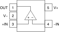
DBV Package
5-Pin SOT-23
Top View

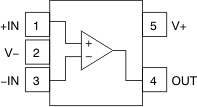
DCK Package
5-Pin SC70
Top View

Pin Functions: TLV316
| PIN | I/O | DESCRIPTION | ||
|---|---|---|---|---|
| NAME | DBV (SOT-23) | DCK (SC70) | ||
| –IN | 4 | 3 | I | Inverting input |
| +IN | 3 | 1 | I | Noninverting input |
| OUT | 1 | 4 | O | Output |
| V– | 2 | 2 | — | Negative (lowest) supply or ground (for single-supply operation) |
| V+ | 5 | 5 | — | Positive (highest) supply |
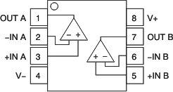
D, DGK Packages
8-Pin SOIC, VSSOP
Top View

Pin Functions: TLV2316
| PIN | I/O | DESCRIPTION | |
|---|---|---|---|
| NO. | NAME | ||
| 2 | –IN A | I | Inverting input, channel A |
| 3 | +IN A | I | Noninverting input, channel A |
| 6 | –IN B | I | Inverting input, channel B |
| 5 | +IN B | I | Noninverting input, channel B |
| 1 | OUT A | O | Output, channel A |
| 7 | OUT B | O | Output, channel B |
| 4 | V– | — | Negative (lowest) supply or ground (for single-supply operation) |
| 8 | V+ | — | Positive (highest) supply |
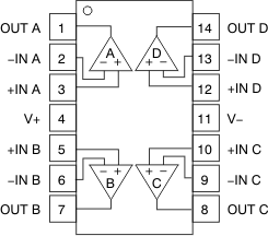
Pin Functions: TLV4316
| PIN | I/O | DESCRIPTION | |
|---|---|---|---|
| NO. | NAME | ||
| 2 | –IN A | I | Inverting input, channel A |
| 3 | +IN A | I | Noninverting input, channel A |
| 6 | –IN B | I | Inverting input, channel B |
| 5 | +IN B | I | Noninverting input, channel B |
| 9 | –IN C | I | Inverting input, channel C |
| 10 | +IN C | I | Noninverting input, channel C |
| 13 | –IN D | I | Inverting input, channel D |
| 12 | +IN D | I | Noninverting input, channel D |
| 1 | OUT A | O | Output, channel A |
| 7 | OUT B | O | Output, channel B |
| 8 | OUT C | O | Output, channel C |
| 14 | OUT D | O | Output, channel D |
| 11 | V– | — | Negative (lowest) supply or ground (for single-supply operation) |
| 4 | V+ | — | Positive (highest) supply |
