ZHCSJ16D November 2018 – June 2022 TLIN1441-Q1
PRODUCTION DATA
- 1 特性
- 2 应用
- 3 说明
- 4 Revision History
- 5 说明(续)
- 6 Pin Configuration and Functions
- 7 Specifications
- 8 Parameter Measurement Information
-
9 Detailed Description
- 9.1 Overview
- 9.2 Functional Block Diagram
- 9.3
Feature Description
- 9.3.1 LIN Pin
- 9.3.2 TXD (Transmit Input)
- 9.3.3 RXD (Receive Output)
- 9.3.4 WAKE (High Voltage Local Wake Up Input)
- 9.3.5 WDT/CLK (Pin Programmable Watchdog Delay Input/SPI Clock)
- 9.3.6 WDI/SDI (Watchdog Timer Input/SPI Serial Data In)
- 9.3.7 PIN/nCS (Pin Watchdog Select/SPI Chip Select)
- 9.3.8 LIMP (LIMP Home output – High Voltage Open Drain Output)
- 9.3.9 nWDR/SDO (Watchdog Timeout Reset Output/SPI Serial Data Out)
- 9.3.10 VSUP (Supply Voltage)
- 9.3.11 GND (Ground)
- 9.3.12 EN/nINT (Enable Input/Interrupt Output in SPI Mode)
- 9.3.13 nRST/nWDR (Reset Output/Watchdog Timeout Reset Output)
- 9.3.14 VCC (Supply Output)
- 9.3.15 Protection Features
- 9.4 Device Functional Modes
- 9.5 Programming
- 9.6 Registers
- 10Application and Implementation
- 11Power Supply Recommendations
- 12Layout
- 13Device and Documentation Support
- 14Mechanical, Packaging, and Orderable Information
8.1 Test Circuit: Diagrams and Waveforms
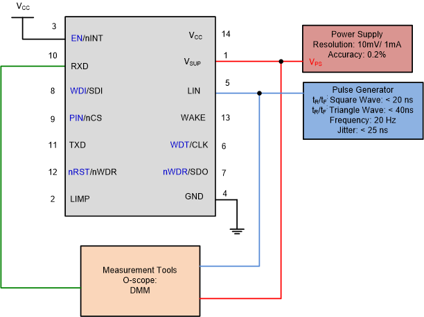 Figure 8-1 Test System: Operating Voltage Range with RX and TX Access
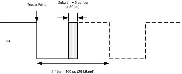 Figure 8-2 RX Response: Operating Voltage Range
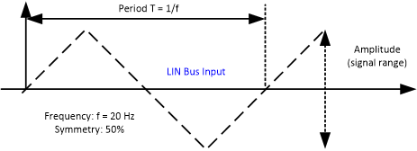 Figure 8-3 LIN Bus Input Signal
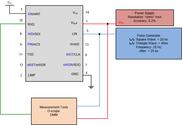 Figure 8-4 LIN Receiver Test with RX access
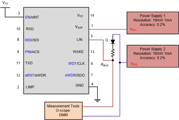 Figure 8-5 VSUP_NON_OP Test Circuit
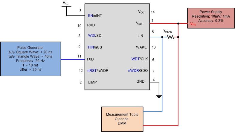 Figure 8-6 Test Circuit for IBUS_LIM at Dominant State (Driver on)
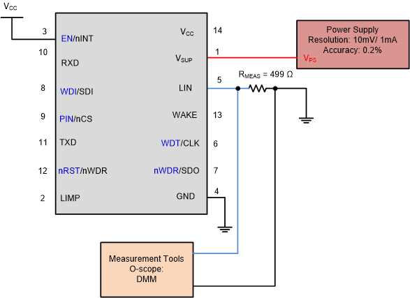 Figure 8-7 Test Circuit for IBUS_PAS_dom; TXD = Recessive State VBUS = 0 V
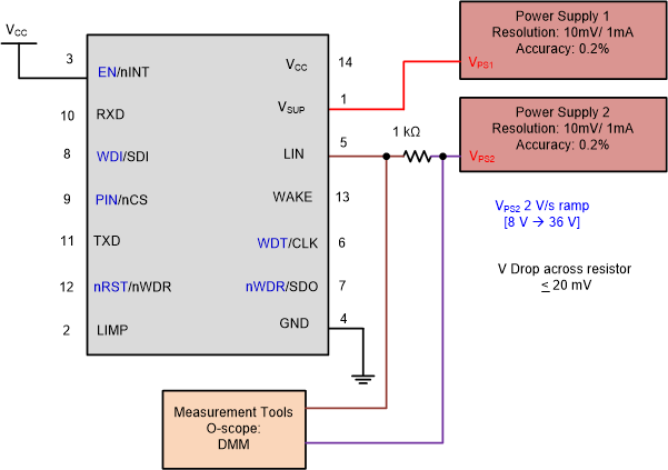 Figure 8-8 Test Circuit for IBUS_PAS_rec
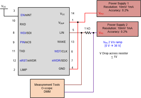 Figure 8-9 Test Circuit for IBUS_NO_GND Loss of GND
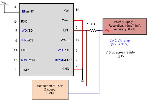 Figure 8-10 Test Circuit for IBUS_NO_BAT Loss of Battery
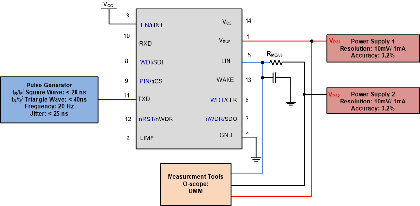 Figure 8-11 Test Circuit Slope Control and Duty Cycle
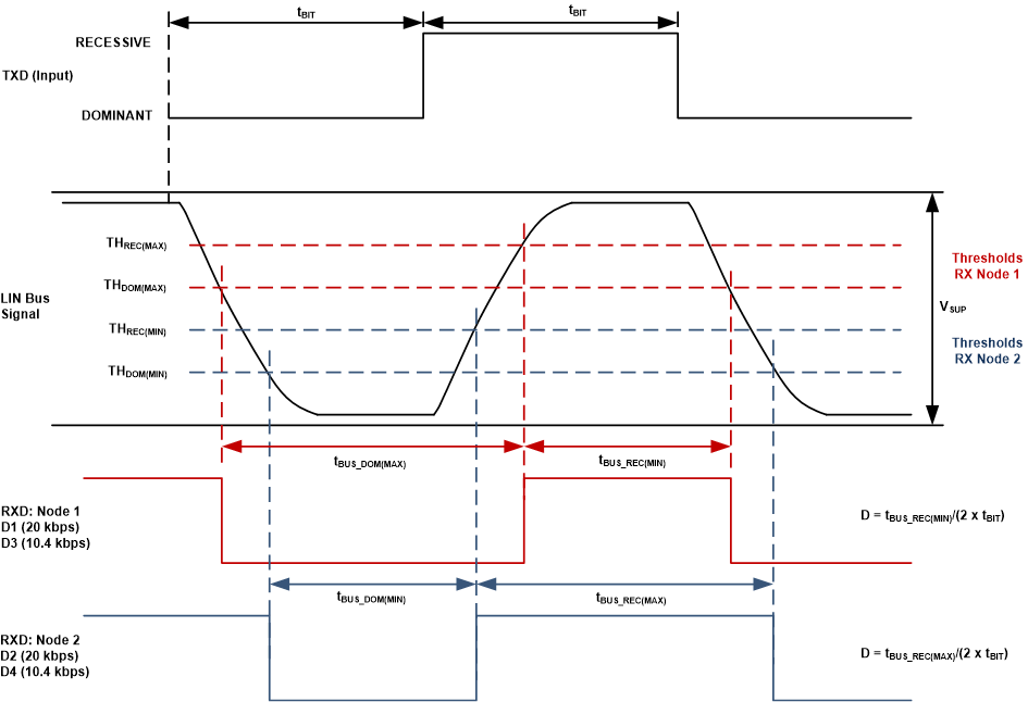 Figure 8-12 Definition of Bus Timing
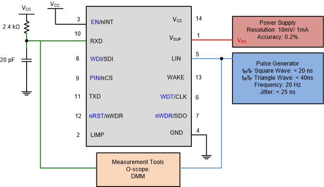 Figure 8-13 Propagation Delay Test Circuit
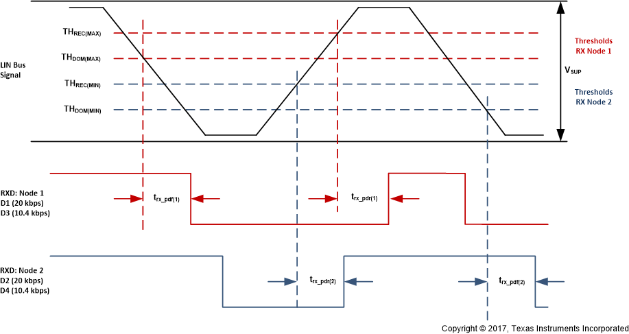 Figure 8-14 Propagation Delay
 Figure 8-15 Mode Transitions
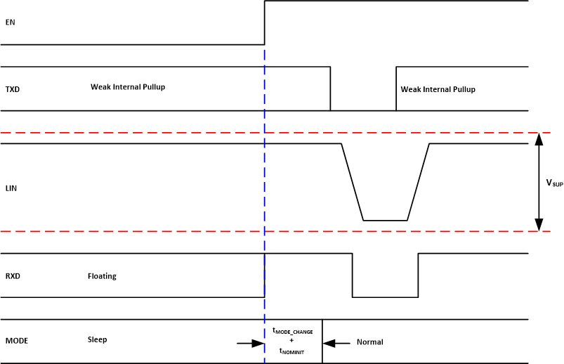 Figure 8-16 Wakeup Through EN
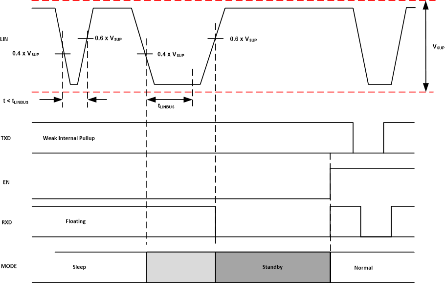 Figure 8-17 Wakeup through LIN
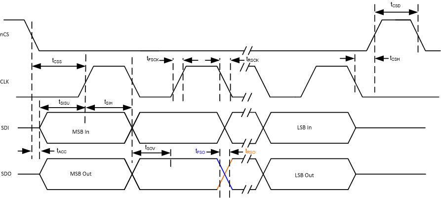 Figure 8-18 SPI AC Characteristic for Read and Write
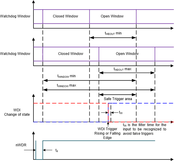 Figure 8-19 Watchdog Window Timing Diagram