ZHCSJY5D June 2019 – June 2022 TLIN1021-Q1
PRODUCTION DATA
- 1 特性
- 2 应用
- 3 说明
- 4 Revision History
- 5 说明(续)
- 6 Pin Configuration and Functions
- 7 Specifications
- 8 Parameter Measurement Information
-
9 Detailed Description
- 9.1 Overview
- 9.2 Functional Block Diagram
- 9.3 Feature Description
- 9.4 Device Functional Modes
- 10Application and Implementation
- 11Device and Documentation Support
- 12Mechanical, Packaging, and Orderable Information
封装选项
机械数据 (封装 | 引脚)
散热焊盘机械数据 (封装 | 引脚)
- DRB|8
订购信息
9.4.4.1 Local Wake-Up (LWU) via WAKE Input Terminal
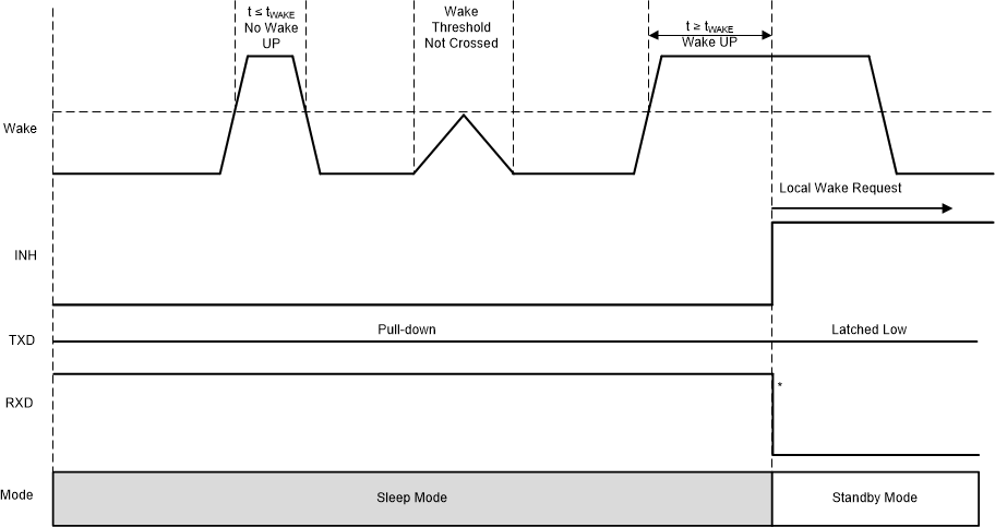
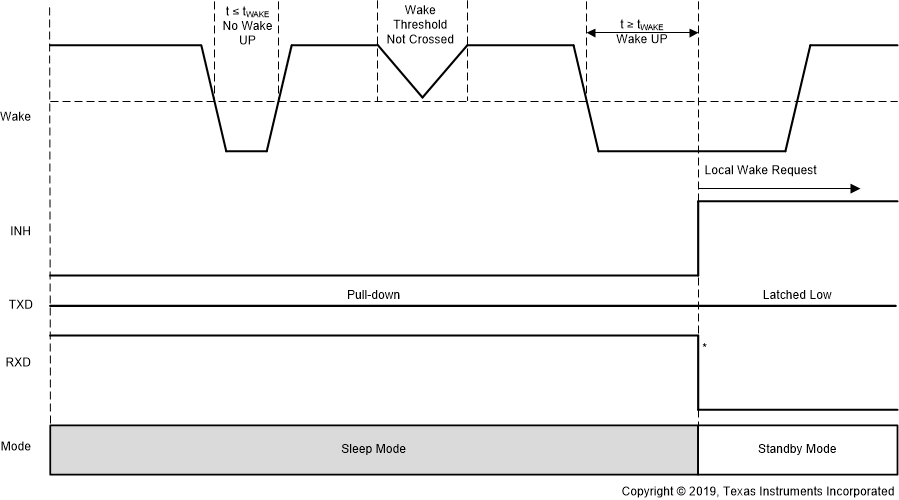
The WAKE terminal is a bi-directional high-voltage input which can be used for local wake-up (LWU) requests via a voltage transition. A LWU event is triggered on either a low-to-high or high-to-low transition since it has bi-directional input thresholds. The WAKE pin could be used with a switch to VSUP or to ground. If the terminal is unused it should be pulled to VSUP or ground to avoid unwanted parasitic wake-up events. When a LWU event takes place the TXD pin is pulled hard to GND letting the LIN controller know that the wake-up event was due to the WAKE pin and not a wake over LIN event.
The LWU circuitry is active in standby mode and sleep mode. If a valid LWU event occurs in standby mode, the device remains in standby mode and drive the RXD output low. If a valid LWU event occurs in sleep mode, the device transitions to standby mode and drive the RXD output low. The LWU circuitry is not active in normal mode. To minimize system level current consumption, the internal bias voltages of the terminal follows the state on the terminal with a delay of tWAKE(MIN). A constant high level on WAKE has an internal pull-up to VSUP, and a constant low level on WAKE has an internal pull-down to GND.
 Figure 9-5 Local Wake-Up – Rising
Edge
 Figure 9-6 Local Wake-Up – Falling
Edge