ZHCSJY5D June   2019  – June 2022 TLIN1021-Q1

PRODUCTION DATA  

  1. 特性
  2. 应用
  3. 说明
  4. Revision History
  5. 说明(续)
  6. Pin Configuration and Functions
  7. Specifications
    1. 7.1 Absolute Maximum Ratings
    2. 7.2 ESD Ratings
    3. 7.3 Thermal Information
    4. 7.4 Recommended Operating Conditions
    5. 7.5 Power Supply Characteristics
    6. 7.6 Electrical Characteristics
    7. 7.7 AC Switching Characteristics
    8. 7.8 Typical Characteristics
  8. Parameter Measurement Information
  9. Detailed Description
    1. 9.1 Overview
    2. 9.2 Functional Block Diagram
    3. 9.3 Feature Description
      1. 9.3.1  LIN
        1. 9.3.1.1 LIN Transmitter Characteristics
        2. 9.3.1.2 LIN Receiver Characteristics
          1. 9.3.1.2.1 Termination
      2. 9.3.2  TXD
      3. 9.3.3  RXD
      4. 9.3.4  VSUP
      5. 9.3.5  GND
      6. 9.3.6  EN
      7. 9.3.7  WAKE
      8. 9.3.8  INH
      9. 9.3.9  Local Faults
      10. 9.3.10 TXD Dominant Time-Out (DTO)
      11. 9.3.11 Bus Stuck Dominant System Fault: False Wake-Up Lockout
      12. 9.3.12 Thermal Shutdown
      13. 9.3.13 Under Voltage on VSUP
      14. 9.3.14 Unpowered Device
    4. 9.4 Device Functional Modes
      1. 9.4.1 Normal Mode
      2. 9.4.2 Sleep Mode
      3. 9.4.3 Standby Mode
      4. 9.4.4 Wake-Up Events
        1. 9.4.4.1 Local Wake-Up (LWU) via WAKE Input Terminal
        2. 9.4.4.2 Wake-Up Request (RXD)
  10. 10Application and Implementation
    1. 10.1 Application Information
    2. 10.2 Typical Application
      1. 10.2.1 Design Requirements
      2. 10.2.2 Detailed Design Procedures
        1. 10.2.2.1 Normal Mode Application Note
        2. 10.2.2.2 TXD Dominant State Time-Out Application Note
      3. 10.2.3 Application Curves
    3. 10.3 Power Supply Recommendations
    4.     Layout
      1. 10.4.1 Layout Guidelines
      2. 10.4.2 Layout Example
  11. 11Device and Documentation Support
    1. 11.1 Documentation Support
      1. 11.1.1 Related Documentation
    2. 11.2 接收文档更新通知
    3. 11.3 支持资源
    4. 11.4 Trademarks
    5. 11.5 Electrostatic Discharge Caution
    6. 11.6 术语表
  12. 12Mechanical, Packaging, and Orderable Information

封装选项

机械数据 (封装 | 引脚)
散热焊盘机械数据 (封装 | 引脚)
订购信息

Application Curves

Figure 10-2 and Figure 10-3 show the propagation delay from the TXD pin to the LIN pin for the dominant to recessive and recessive to dominant edges.
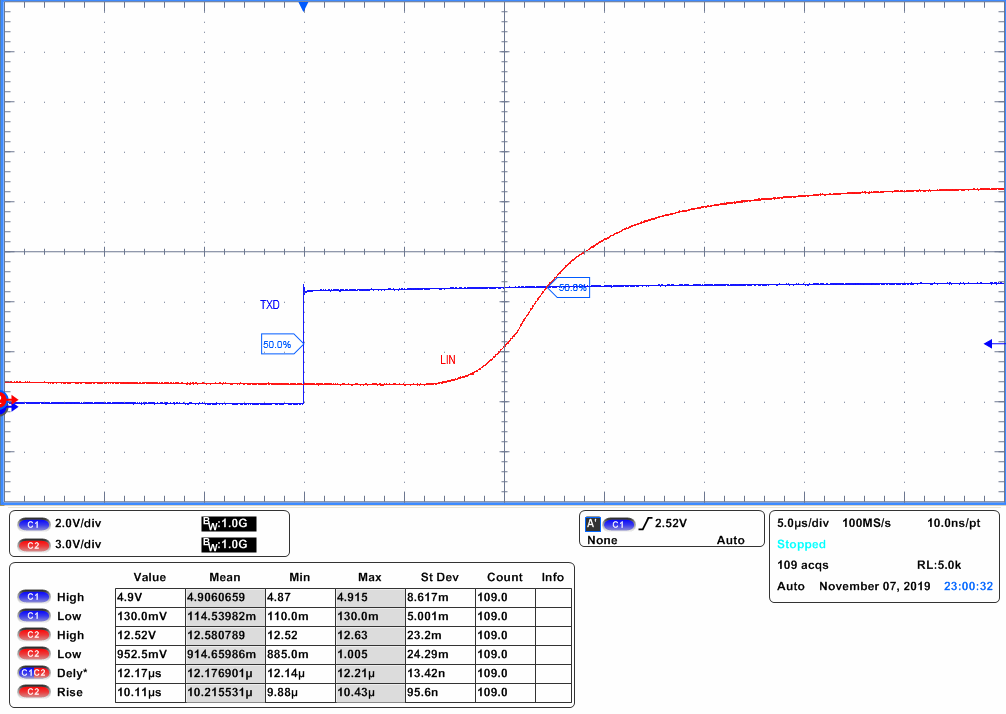
GUID-AC05FCF0-B52D-40ED-91E3-96E7E583E883-low.gifFigure 10-2 Dominant To Recessive Propagation Delay
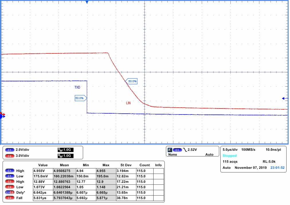
GUID-783B4C12-46B3-455E-B20F-4AA27228264E-low.gifFigure 10-3 Recessive to Dominant Propagation Delay